Altera Stratix IV GX FPGA Development Board User Manual
Page 69
Chapter 2: Board Components
2–61
Memory
August 2012
Altera Corporation
Stratix IV GX FPGA Development Board
Reference Manual
This 16-bit data memory interface can sustain burst read operations at up to 52 MHz
for a throughput of 832 Mbps. The write performance is 125 µs for a single word and
440 µs for a 32-word buffer. The erase time is 400 ms for a 32 K parameter block and
1200 ms for a 128 K main block.
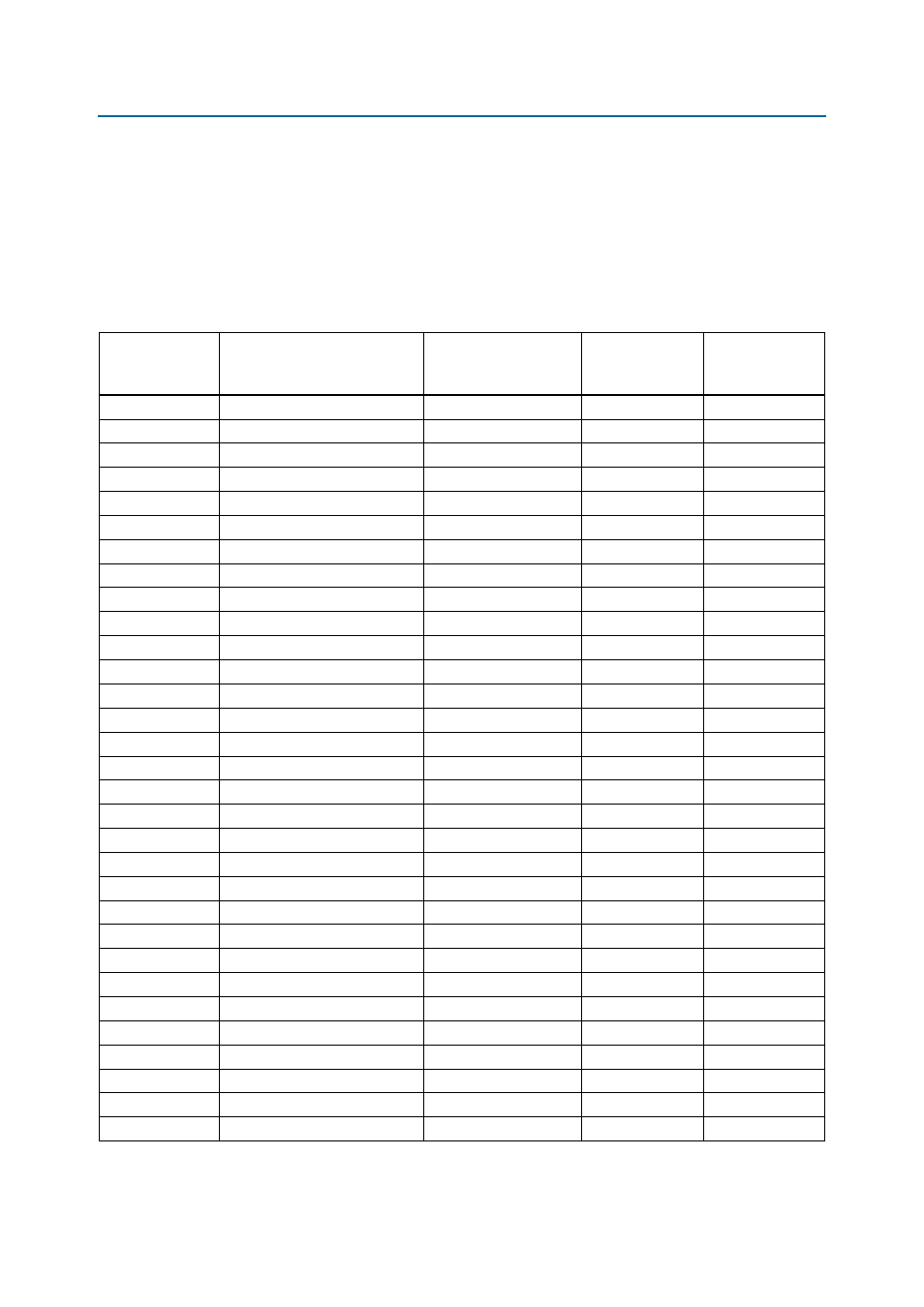
lists the flash pin assignments, signal names, and functions. The signal
names and types are relative to the Stratix IV GX device in terms of I/O setting and
direction.
Table 2–56. Flash Pin Assignments, Schematic Signal Names, and Functions (Part 1 of 2)
Board Reference
Description
Schematic Signal Name
I/O Standard
Stratix IV GX
Device
Pin Number
U32.B6
Address bus (die select)
FSM_A25
2.5-V
AP30
U32.H8
Address bus
FSM_A24
2.5-V
AN30
U32.G1
Address bus
FSM_A23
2.5-V
AL31
U32.A8
Address bus
FSM_A22
2.5-V
AK31
U32.C8
Address bus
FSM_A21
2.5-V
AR32
U32.C7
Address bus
FSM_A20
2.5-V
AP32
U32.B7
Address bus
FSM_A19
2.5-V
AH29
U32.A7
Address bus
FSM_A18
2.5-V
AG29
U32.D8
Address bus
FSM_A17
2.5-V
AR35
U32.D7
Address bus
FSM_A16
2.5-V
AP35
U32.C5
Address bus
FSM_A15
2.5-V
AL32
U32.B5
Address bus
FSM_A14
2.5-V
AK32
U32.A5
Address bus
FSM_A13
2.5-V
AU33
U32.C4
Address bus
FSM_A12
2.5-V
AT33
U32.D3
Address bus
FSM_A11
2.5-V
AH30
U32.C3
Address bus
FSM_A10
2.5-V
AJ31
U32.B3
Address bus
FSM_A9
2.5-V
AR34
U32.A3
Address bus
FSM_A8
2.5-V
AT34
U32.C2
Address bus
FSM_A7
2.5-V
AE27
U32.A2
Address bus
FSM_A6
2.5-V
AD27
U32.D2
Address bus
FSM_A5
2.5-V
AP34
U32.D1
Address bus
FSM_A4
2.5-V
AN33
U32.C1
Address bus
FSM_A3
2.5-V
AD26
U32.B1
Address bus
FSM_A2
2.5-V
AC26
U32.A1
Address bus
FSM_A1
2.5-V
AP33
U32.E7
Data bus
FSM_D16
2.5-V
C33
U32.G7
Data bus
FSM_D15
2.5-V
N31
U32.H5
Data bus
FSM_D14
2.5-V
M31
U32.F5
Data bus
FSM_D13
2.5-V
C32
U32.F4
Data bus
FSM_D12
2.5-V
B32
U32.F3
Data bus
FSM_D11
2.5-V
J32