Clock circuitry, Stratix iv gx fpga clock inputs, Clock circuitry –22 – Altera Stratix IV GX FPGA Development Board User Manual
Page 30: Stratix iv gx fpga clock inputs –22
2–22
Chapter 2: Board Components
Clock Circuitry
Stratix IV GX FPGA Development Board
August 2012
Altera Corporation
Reference Manual
Clock Circuitry
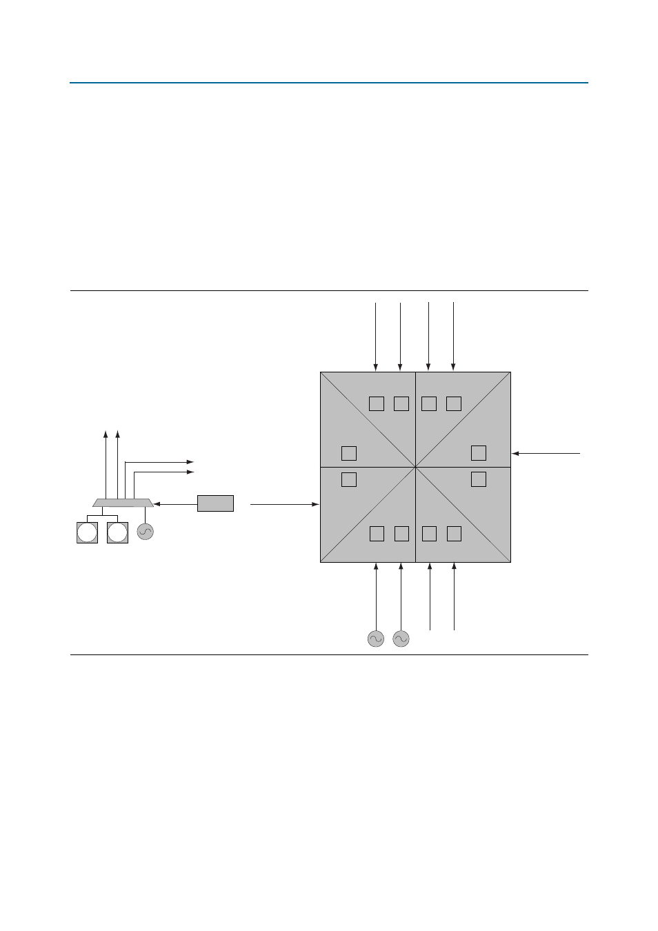
This section describes the board's clock inputs and outputs.
Stratix IV GX FPGA Clock Inputs
The development board has two types of clock inputs: global clock inputs and
transceiver reference clock inputs.
shows the Stratix IV GX FPGA development board global clock inputs. The
Stratix IV GX FPGA development board transceiver reference clock inputs are shown
in
.
Figure 2–6. Stratix IV GX FPGA Development Board Global Clock Inputs
B1
B2
B3
B4
B6
B5
B8
B7
CLK2p
CLK3p
CLKIN_50
HS
MA
_CLK
_IN0
2.
5V
, NO
O
C
T
2.
5V
, N
O
OC
T
REFCLK INPUT
SMA
SMA
LVPECL or
Single-Ended
2-to-4 buffer
100 M*
CLK_SEL
CLK
INR
T
_100_P
CLK
IN
LT
_100_P
CLKINTOP_100_P
CLKINBOT_100_P
DIPSW
SW4-5
To REFCLK
Clock Inputs
CLK1p
CLK0p
CLK9p
CLK8p
CLK
10p
CLK
11p
CLK7p
CLK6p
CLK4p
CLK5p
CLK13p
CLK12p
CLK14p
CLK15p
PLL
B2
PLL
B1
PLL
T2
PLL
T1
PLL
L3
PLL
L4
PLL
L1
PLL
L2
PLL
R3
PLL
R4
PLL
R1
PLL
R2
HS
MA
_CLK
_IN_P
2
LV
DS
, O
C
T
100
Ω
CLK
_125_P
LV
D
S
, D
iffe
re
nti
al
OC
T
HS
MB
_CLK
_IN0
2.
5V
, NO
O
C
T
CLKINBOT_100_P
LVDS, Differential OCT
HS
MA
_CLK
_IN_P
1
LV
DS
, O
C
T
100
Ω
HS
MB
_CLK
_IN_P
1
LV
DS
, O
C
T
100
Ω
HS
MB
_CLK
_IN_P
2
LV
DS
, O
C
T
100
Ω
CLKINTOP_100_P
LVDS, Differential OCT
*The 100 MHz oscillator (X6) can be programmed
to any frequency between 10 MHz and 800 MHz
but powers up to 100 MHz using the clock control
GUI installed with the kit CD.