Lcd –30 – Altera Stratix IV GX FPGA Development Board User Manual
Page 38
2–30
Chapter 2: Board Components
General User Input/Output
Stratix IV GX FPGA Development Board
August 2012
Altera Corporation
Reference Manual
LCD
The development board contains a single 14-pin 0.1" pitch dual-row header that
interfaces to a 16 character × 2 line Lumex LCD display. The LCD has a 14-pin
receptacle that mounts directly to the board's 14-pin header, so it can be easily
removed for access to components under the display. You can also use the header for
debugging or other purposes.
summarizes the LCD pin assignments. The signal names and directions are
relative to the Stratix IV GX FPGA.
shows the LCD pin definitions, and is an excerpt from the Lumex data
sheet.
f
For more information such as timing, character maps, interface guidelines, and other
related documentation, visi
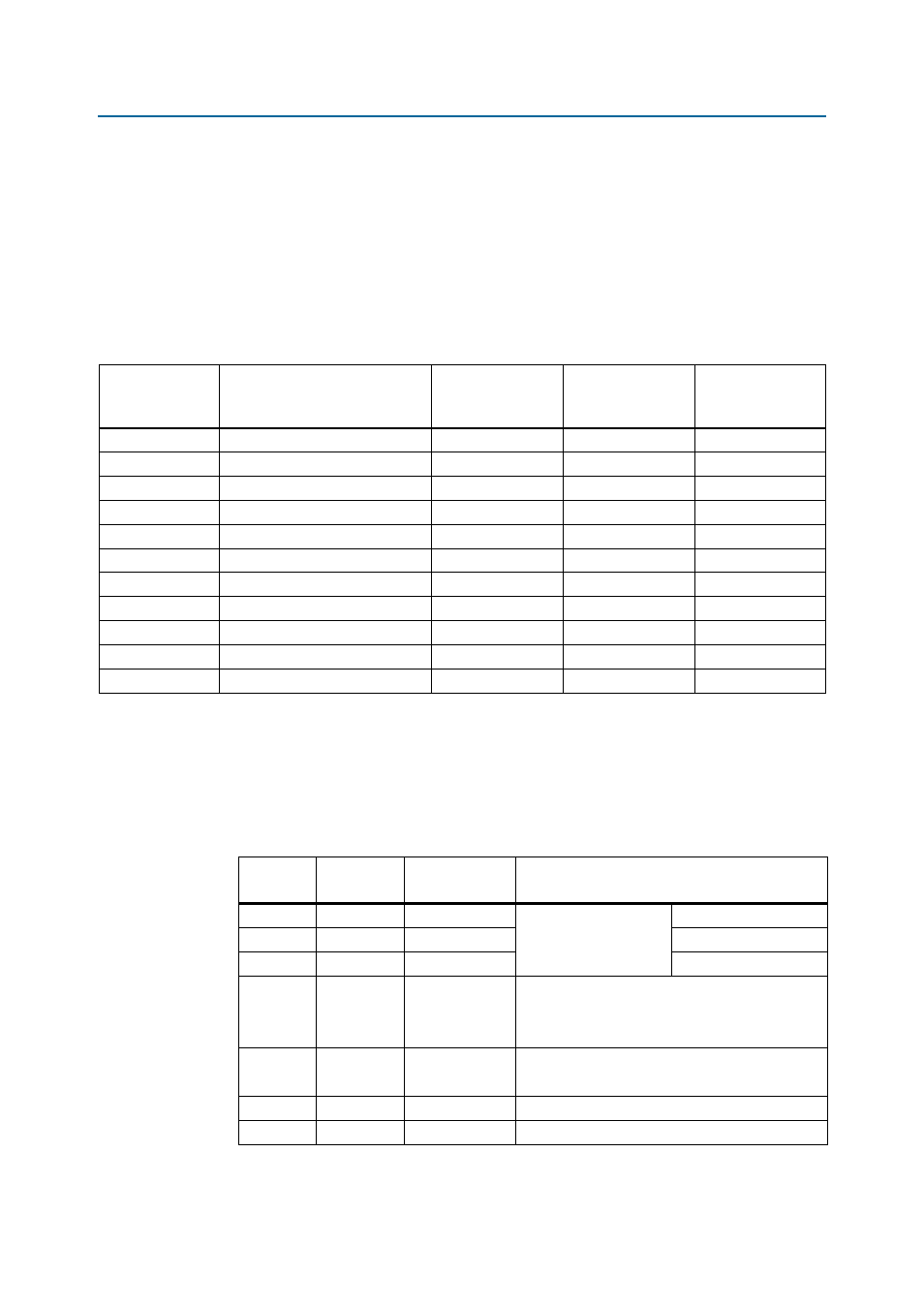
Table 2–31. LCD Pin Assignments, Schematic Signal Names, and Functions
Board Reference
Description
Schematic Signal
Name
I/O Standard
Stratix IV GX
Device
Pin Number
J16.7
LCD data bus
LCD_DATA0
2.5-V
AD31
J16.8
LCD data bus
LCD_DATA1
2.5-V
AJ34
J16.9
LCD data bus
LCD_DATA2
2.5-V
R31
J16.10
LCD data bus
LCD_DATA3
2.5-V
L32
J16.11
LCD data bus
LCD_DATA4
2.5-V
T30
J16.12
LCD data bus
LCD_DATA5
2.5-V
AN34
J16.13
LCD data bus
LCD_DATA6
2.5-V
T31
J16.14
LCD data bus
LCD_DATA7
2.5-V
AD30
J16.4
LCD data or command select
LCD_D_Cn
2.5-V
AB30
J16.5
LCD write enable
LCD_Wen
2.5-V
AL34
J16.6
LCD chip select
LCD_CSn
2.5-V
K34
Table 2–32. LCD Pin Definitions and Functions
Pin
Number
Symbol
Level
Function
1
V
DD
—
Power supply
5 V
2
V
SS
—
GND (0 V)
3
V
0
—
For LCD drive
4
RS
H/L
Register select signal
H: Data input
L: Instruction input
5
R/W
H/L
H: Data read (module to MPU)
L: Data write (MPU to module)
6
E
H, H to L
Enable
7–14
DB0–DB7
H/L
Data bus, software selectable 4-bit or 8-bit mode