Qdrii+ top port 1, Qdrii+ top port 1 –55 – Altera Stratix IV GX FPGA Development Board User Manual
Page 63
Chapter 2: Board Components
2–55
Memory
August 2012
Altera Corporation
Stratix IV GX FPGA Development Board
Reference Manual
lists the QDRII+ top port 0 component reference and manufacturing
information.
QDRII+ Top Port 1
The QDRII+ top port 1 consists of a single QDRII+ burst-of-4 SRAM, providing
4 Mbyte with an 18-bit read data bus and an 18-bit write data bus.
This memory interface is designed to run between 120 MHz, the minimum frequency
for this device, and 400 MHz for a maximum theoretical bandwidth of over 14.4 Gbps
for reading and 14.4 Gbps for writing. The internal bus in the FPGA is typically 2 or 4
times the width at full rate or half rate respectively. For example, a 400 MHz 18-bit
interface becomes a 200 MHz 72 bit bus.
U22.K3
Read data bus
QDR2TOP0_Q14
1.5-V HSTL Class I
P25
U22.G3
Read data bus
QDR2TOP0_Q13
1.5-V HSTL Class I
G27
U22.F2
Read data bus
QDR2TOP0_Q12
1.5-V HSTL Class I
F27
U22.E3
Read data bus
QDR2TOP0_Q11
1.5-V HSTL Class I
D28
U22.D3
Read data bus
QDR2TOP0_Q10
1.5-V HSTL Class I
E28
U22.B2
Read data bus
QDR2TOP0_Q9
1.5-V HSTL Class I
D29
U22.B11
Read data bus
QDR2TOP0_Q8
1.5-V HSTL Class I
E29
U22.C10
Read data bus
QDR2TOP0_Q7
1.5-V HSTL Class I
F28
U22.E11
Read data bus
QDR2TOP0_Q6
1.5-V HSTL Class I
G29
U22.F11
Read data bus
QDR2TOP0_Q5
1.5-V HSTL Class I
J26
U22.J10
Read data bus
QDR2TOP0_Q4
1.5-V HSTL Class I
K26
U22.K11
Read data bus
QDR2TOP0_Q3
1.5-V HSTL Class I
J27
U22.L11
Read data bus
QDR2TOP0_Q2
1.5-V HSTL Class I
L26
U22.M10
Read data bus
QDR2TOP0_Q1
1.5-V HSTL Class I
K28
U22.P11
Read data bus
QDR2TOP0_Q0
1.5-V HSTL Class I
M27
U22.A11
Read clock P
QDR2TOP0_CQ_P
1.5-V HSTL Class I
H28
U22.A1
Read clock N
QDR2TOP0_CQ_N
1.5-V HSTL Class I
K27
U22.A8
Read port select
QDR2TOP0_RPSn
1.5-V HSTL Class I
C27
U22.P6
Read data valid
QDR2TOP0_QVLD
1.5-V HSTL Class I
H26
U22.H1
DLL enable
QDR2TOP0_DOFFn
1.5-V HSTL Class I
B22
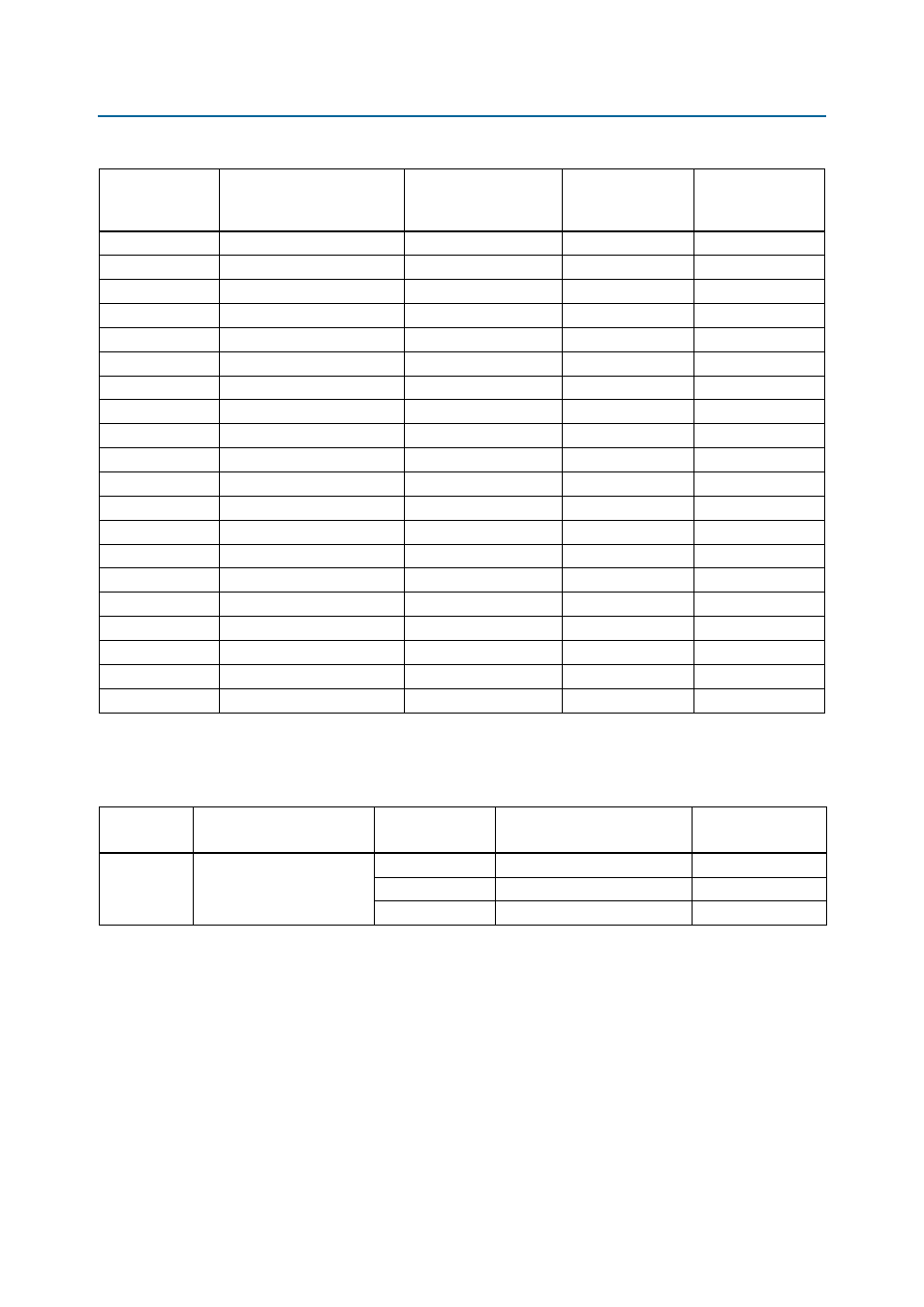
Table 2–50. QDRII+ Top Port 0 Pin Assignments, Signal Names and Functions (Part 3 of 3)
Board Reference
Description
Schematic Signal Name
I/O Standard
Stratix IV GX
Device
Pin Number
Table 2–51. QDRII+ Top Port 0 Component Reference and Manufacturing Information
Board
Reference
Description
Manufacturer
Manufacturing
Part Number
Manufacturer
Website
U22
QDRII+, 4 M × 18, 400 MHZ
Cypress
CY7C2563KV18-400BZXC
NEC
uPD44647186AF5-E22-FQ1
Samsung
K7S3218U4C-EC40