Sdi video input/output, Sdi video input/output –45 – Altera Stratix IV GX FPGA Development Board User Manual
Page 53
Chapter 2: Board Components
2–45
Components and Interfaces
August 2012
Altera Corporation
Stratix IV GX FPGA Development Board
Reference Manual
SDI Video Input/Output
The SDI video port consists of a LMH0302SQ cable driver and a LMH0344 receiver
cable equalizer. The PHY devices from National Semiconductor interface to
single-ended 75-
Ω SMB connectors and extends out through the PCI Express bracket
for easy use while installed in a host PC.
The LMH0302SQ driver supports operation at 270 Mbit standard definition (SD),
1.5 Gbit high definition (HD), and 3.0 Gbit dual-link HD modes. Control signals for
SD and HD modes selections, as well as device enable can be set. The device can be
clocked by the 148.5 MHz voltage-controlled crystal oscillator (VCXO) and matched
to incoming signals within 50 ppm using the UP and DN voltage control lines to the
VCXO.
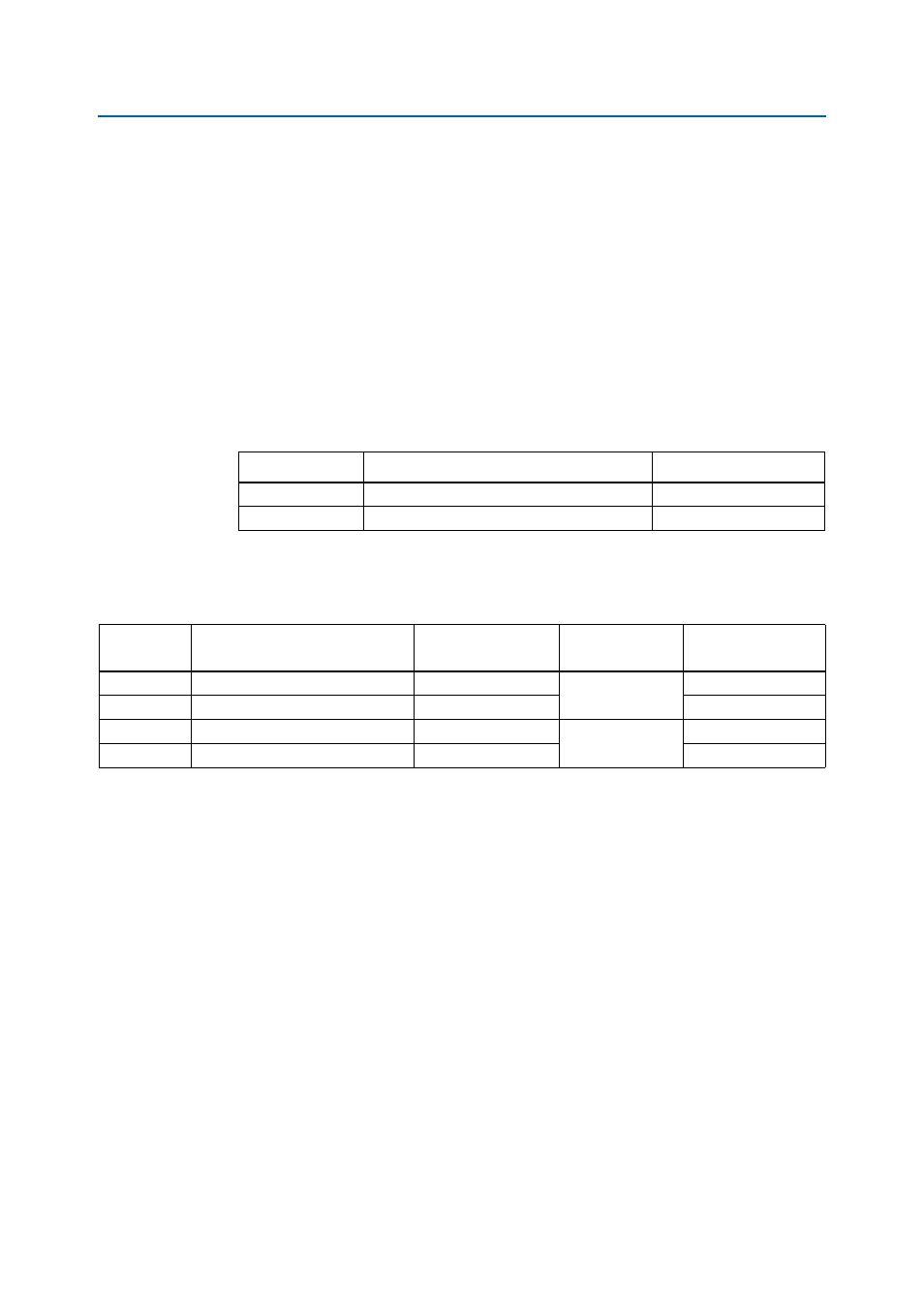
lists the supported output standards for the SD and HD input.
lists the SDI video output interface pin assignments. The signal names and
directions are relative to the Stratix IV GX FPGA.
Table 2–42. Supported Output Standards for SD and HD Input
SD_HD Input
Supported Output Standards
Rise TIme
0
SMPTE 424M, SMPTE 292M
Faster
1
SMPTE 259M
Slower
Table 2–43. SDI Video Output Interface Pin Assignments, Schematic Signal Names, and Functions
Board
Reference
Description
Schematic
Signal Name
I/O Standard
Stratix IV GX Device
Pin Number
U4.1
SDI video output P
SDI_TX_P
1.4-V PCML
K4
U4.2
SDI video output N
SDI_TX_N
K3
U4.6
Device enable
SDI_TX_EN
2.5-V
N6
U4.10
High definition select
SDI_TX_SD_HDn
V29