Altera Stratix IV GX FPGA Development Board User Manual
Page 43
Chapter 2: Board Components
2–35
Components and Interfaces
August 2012
Altera Corporation
Stratix IV GX FPGA Development Board
Reference Manual
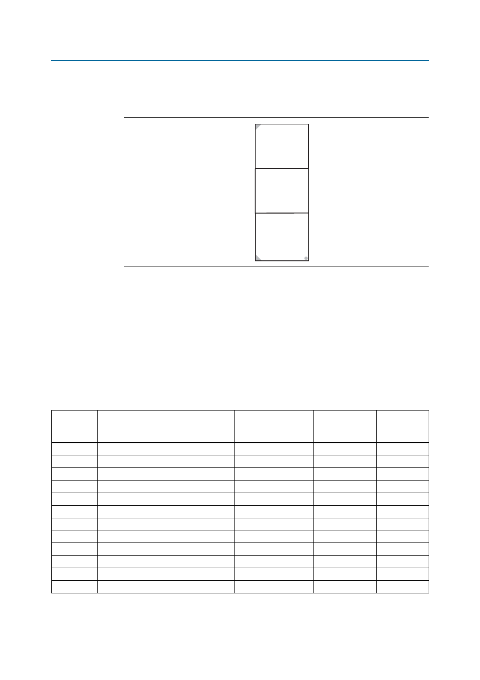
shows the bank arrangement of signals with respect to the Samtec
connector's three banks.
The HSMC interface has programmable bi-directional I/O pins that can be used as
2.5-V LVCMOS, which is 3.3-V LVTTL-compatible. These pins can also be used as
various differential I/O standards including, but not limited to, LVDS, mini-LVDS,
and RSDS with up to 17 full-duplex channels.
1
As noted in the
manual, LVDS and
single-ended I/O standards are only guaranteed to function when mixed according to
either the generic single-ended pin-out or generic differential pin-out.
lists the HSMC port A interface pin assignments, signal names, and
functions.
Figure 2–11. HSMC Signal and Bank Diagram
Bank 3
Power
D(79.40)
-or-
LVDS
CLKIN2, CLKOUT2
Bank 2
Power
D(39:0)
-or-
D[3:0] + LVDS
CLKIN1, CLKOUT1
Bank 1
8 TX Channels CDR
8 RX Channels CDR
JTAG
SMB
CLKIN0, CLKOUT0
Table 2–37. HSMC Port A Pin Assignments, Schematic Signal Names, and Functions (Part 1 of 4)
Board
Reference
Description
Schematic Signal
Name
I/O Standard
Stratix IV GX
Device
Pin Number
J1.1
Transceiver TX bit 7
HSMA_TX_P7
1.4-V PCML
P4
J1.2
Transceiver RX bit 7
HSMA_RX_P7
1.4-V PCML
R2
J1.3
Transceiver TX bit 7n
HSMA_TX_N7
1.4-V PCML
P3
J1.4
Transceiver RX bit 7n
HSMA_RX_N7
1.4-V PCML
R1
J1.5
Transceiver TX bit 6
HSMA_TX_P6
1.4-V PCML
T4
J1.6
Transceiver RX bit 6
HSMA_RX_P6
1.4-V PCML
U2
J1.7
Transceiver TX bit 6n
HSMA_TX_N6
1.4-V PCML
T3
J1.8
Transceiver RX bit 6n
HSMA_RX_N6
1.4-V PCML
U1
J1.9
Transceiver TX bit 5
HSMA_TX_P5
1.4-V PCML
AB4
J1.10
Transceiver RX bit 5
HSMA_RX_P5
1.4-V PCML
AC2
J1.11
Transceiver TX bit 5n
HSMA_TX_N5
1.4-V PCML
AB3
J1.12
Transceiver RX bit 5n
HSMA_RX_N5
1.4-V PCML
AC1