Reset configuration push button, Rotary switch – Altera Stratix IV GX FPGA Development Board User Manual
Page 28
2–20
Chapter 2: Board Components
Configuration, Status, and Setup Elements
Stratix IV GX FPGA Development Board
August 2012
Altera Corporation
Reference Manual
lists the PCI Express control DIP switch component reference and
manufacturing information.
Reset Configuration Push Button
The reset configuration push button, RESET_CONFIGn, is an input to the MAX
II CPLD
EPM2210 System Controller. The push button forces a reconfiguration of the FPGA
from flash memory. The location in the flash memory is based on the input from the
rotary switch position when you release the push button. Valid locations include 0
and 1 for the two pages in flash reserved for FPGA designs.
lists the reset configuration push button component reference and
manufacturing information.
Rotary Switch
The 16-position rotary switch (SW2) is wired to the MAX
II CPLD EPM2210 System
Controller. This rotary switch serves the following purposes:
■
At power up or when you press the reset configuration push button (S1), this
switch selects either the factory (page 0) or the user (page 1) design to load into the
FPGA.
■
After power up, the rotary switch selects the power rail monitored from among a
total of 16 rails. The power information is displayed in the Power GUI on a host PC
with a USB connection to the board.
■
User applications can obtain the switch value by reading the rsr register over the
FSM bus in the MAX
II CPLD EPM2210 System Controller.
lists the power rails that are measured based on the rotary switch position.
Table 2–16. PCI Express Control DIP Switch Component Reference and Manufacturing Information
Board Reference
Description
Manufacturer
Manufacturer
Part Number
Manufacturer Website
SW5
Four-Position slide
DIP switch
C & K Components
TDA04H0SB1
Table 2–17. Reset Configuration Push Button Component Reference and Manufacturing Information
Board Reference
Description
Manufacturer
Manufacturer
Part Number
Manufacturer
Website
S1
Push button
Panasonic Corporation
EVQPAC07K
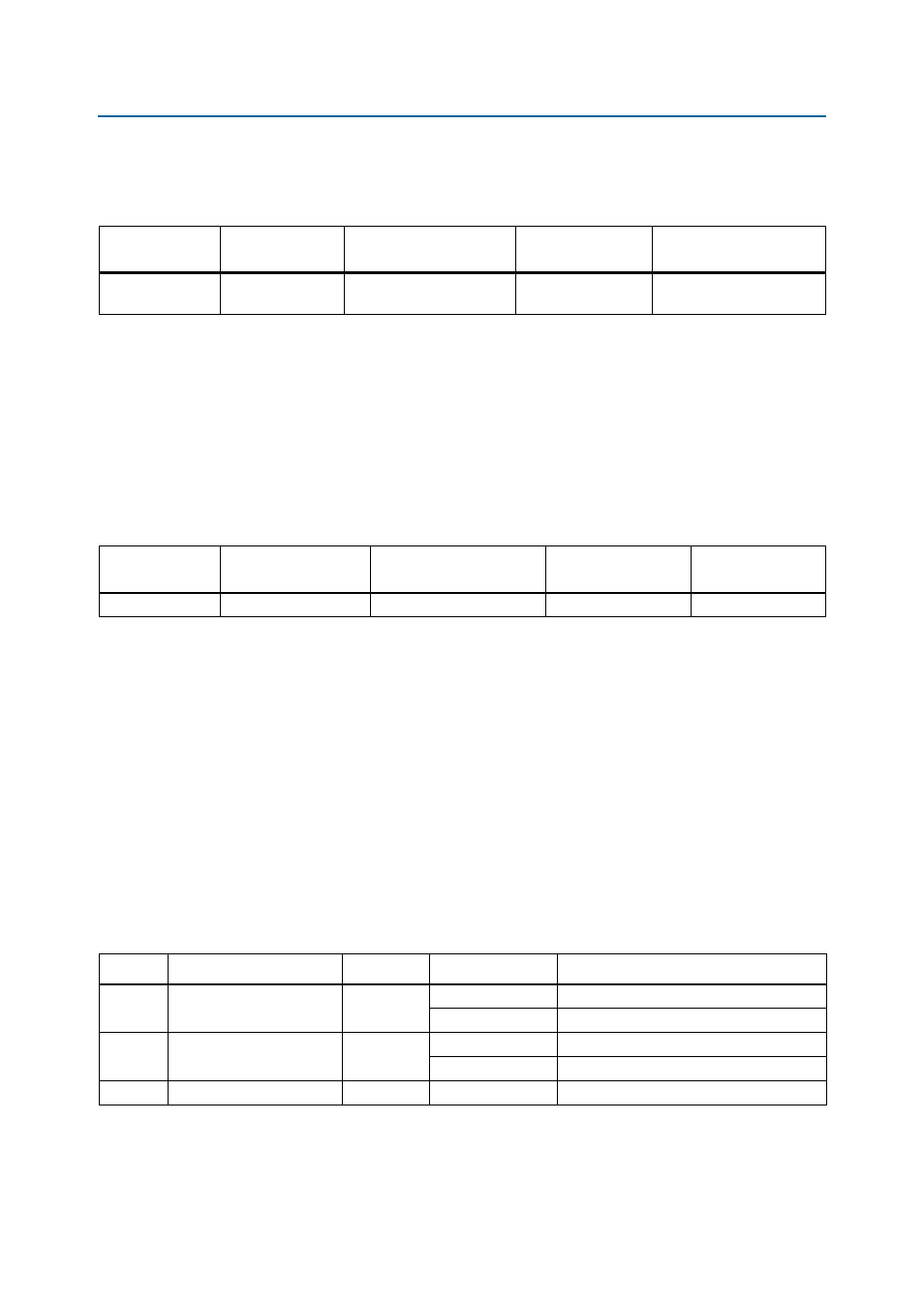
Table 2–18. Power Rail Measurements Based on the Rotary Switch Position (Part 1 of 2)
Switch
Schematic Signal Name
Voltage (V)
Device Pin
Description
0
S4VCCIO_B7B8
1.5
VCCIO_B7
Bank 7 I/O power (QDR2TOP0+DDR)
VCCIO_B8
Bank 8 I/O power (QDR2TOP1+DDR)
1
S4VCC
0.90
VCC
FPGA core and periphery power
VCCHIP
PCI Express hard IP block
2
3.3 V
3.3
—
All 3.3 V power to board (mA only)