Fpga programming over external usb-blaster, Fpga programming over external usb-blaster –16 – Altera Stratix IV GX FPGA Development Board User Manual
Page 24
2–16
Chapter 2: Board Components
Configuration, Status, and Setup Elements
Stratix IV GX FPGA Development Board
August 2012
Altera Corporation
Reference Manual
There are two pages reserved for the FPGA configuration data. The factory hardware
page (page 0) loads if the rotary switch is in position 0 and when either power is
cycled or the reset configuration push button (S1) is pressed. The user hardware page
(page 1) loads if the rotary switch is in position 1 and when either power is cycled or
the reset configuration push button (S1) is pressed.
FPGA Programming over External USB-Blaster
The JTAG programming header provides another method for configuring the FPGA
(U13) using an external USB-Blaster device with the Quartus II Programmer running
on a PC. The external USB-Blaster connects to the board through the JTAG connector
(J8). The JTAG DIP switch (SW6) allows the MAX II CPLD device to be removed from
the JTAG chain so that the FPGA is the only device on the JTAG chain.
f
For more information on the following topics, refer to the respective documents:
■
Board Update Portal, re
.
■
PFL design, refer to the
■
PFL megafunction, refer to
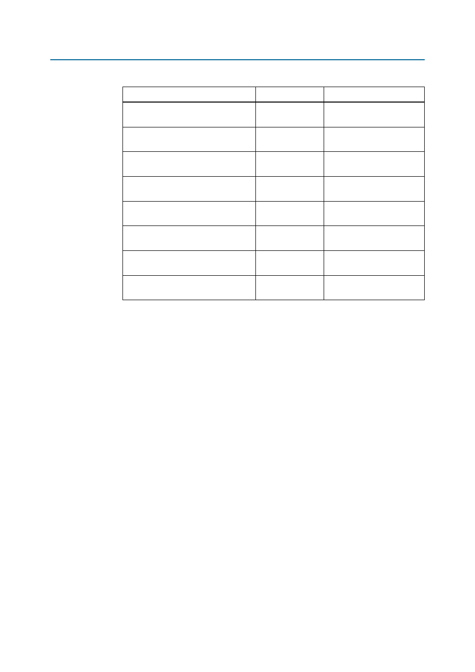
Factory Software
8,192
0x0281.FFFF
0x0202.0000
zipfs — HTML, Web Content
8,192
0x0201.FFFF
0x0182.0000
User Hardware
12,288
0x0181.FFFF
0x00C2.0000
Factory Hardware
12,288
0x00C1.FFFF
0x0002.0000
PFL Option Bits
32
0x0001.FFFF
0x0001.8000
Board Information
32
0x0001.7FFF
0x0001.0000
Ethernet Option Bits
32
0x0000.FFFF
0x0000.8000
User Design Reset Vector
32
0x0000.7FFF
0x0000.0000
Table 2–8. Flash Memory Map (Part 2 of 2)
Name
Size (Kbyte)
Address