Components and interfaces, Pci express, Components and interfaces –31 – Altera Stratix IV GX FPGA Development Board User Manual
Page 39: Pci express –31
Chapter 2: Board Components
2–31
Components and Interfaces
August 2012
Altera Corporation
Stratix IV GX FPGA Development Board
Reference Manual
1
The particular model on this board does not have a backlight and the LCD drive pin is
not connected.
lists the LCD component references and the manufacturing information.
Components and Interfaces
This section describes the development board communication ports and interface
cards relative to the Stratix IV GX device. The development board supports the
following communication ports:
■
PCI Express
■
10/100/1000 Ethernet
■
HSMC
PCI Express
The Stratix IV GX FPGA development board is designed to fit entirely into a PC
motherboard with a ×8 or ×16 PCI Express slot that can accommodate a full height
short form factor add-in card. This interface uses the Stratix IV GX device's PCI
Express hard IP block, saving logic resources for the user logic application.
f
For more information on using the PCI Express hard IP block, refer to
.
The PCI Express interface supports auto-negotiating channel width from ×1 to ×4 to
×8 as well as the connection speed of Gen1 at 2.5 Gbps/lane to Gen2 at 5.0 Gbps/lane
for a maximum of 40 Gbps full-duplex. The PCI Express control DIP switch allows the
presence detect grounding to be altered to enable a ×1, ×4, or ×8 width edge
connector.
The power for the board can be sourced entirely from the PCI Express edge connector
when installed into a PC motherboard. Although the board can also be powered by a
laptop power supply for use on a lab bench, it is not recommended to power from
both supplies at the same time. Ideal diode power sharing devices have been
designed into this board to prevent damages or back-current from one supply to the
other.
The PCIE_REFCLK_P signal is a 100-MHz differential input that is driven from the PC
motherboard on this board through the edge connector. This signal is connected
directly to a Stratix IV GX REFCLK input pin pair using DC coupling. This clock is
terminated on the motherboard and therefore, no on-board termination is required.
This clock can have spread-spectrum properties that change its period between
9.847 ps to 10.203 ps. The I/O standard is High-Speed Current Steering Logic (HCSL).
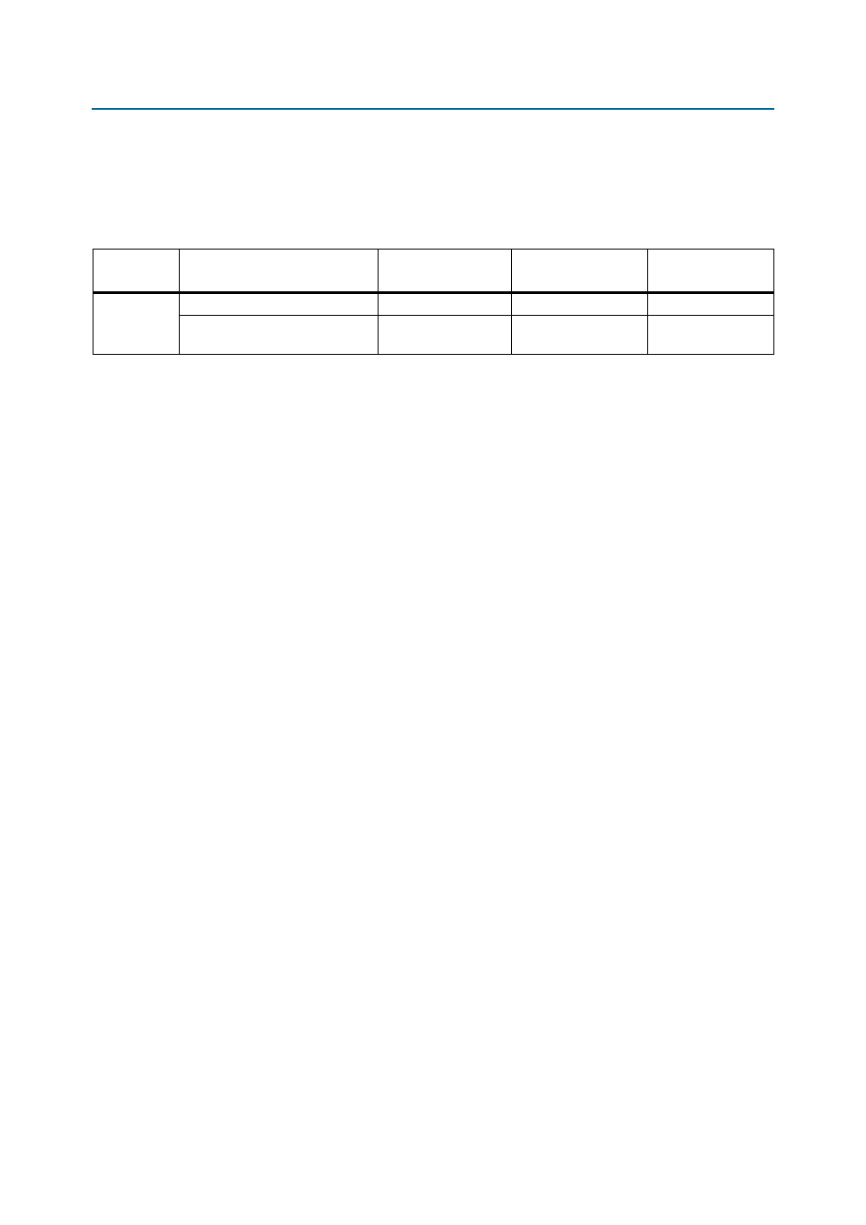
Table 2–33. LCD Component References and Manufacturing Information
Board
Reference
Description
Manufacturer
Manufacturer
Part Number
Manufacturer
Website
J16
2×7 pin, 100 mil, vertical header
Samtec
TSM-107-01-G-DV
2×16 character display, 5×8 dot
matrix
Lumex Inc.
LCM-S01602DSR/C