Altera Stratix IV GX FPGA Development Board User Manual
Page 12
2–4
Chapter 2: Board Components
Board Overview
Stratix IV GX FPGA Development Board
August 2012
Altera Corporation
Reference Manual
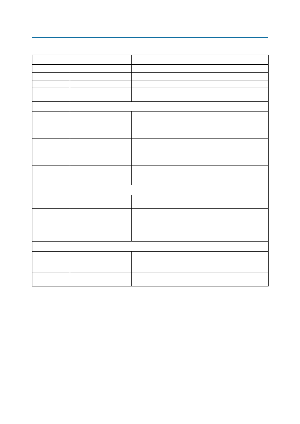
U22
QDRII+ x18/x18 top port 0
18-bit read and 18-bit write 4-MB SRAM port.
U7
QDRII+ x18/x18 top port 1
Second 18-bit read and 18-bit write 4-MB SRAM port.
U30
SSRAM x36 memory
Standard synchronous RAM which makes a 36-bit 2-MB SRAM port.
U32
Flash x16 memory
Synchronous burst mode flash device which provides a 16-bit 64-MB
non-volatile memory port.
Communication Ports
J17
PCI Express edge connector
Connector with gold-plated edge fingers for up to ×8 signaling in either
Gen1 or Gen2 mode.
J1
HSMC port A
Provides eight transceiver channels and 84 CMOS or 17 LVDS
channels per the HSMC specification.
J2
HSMC port B
Provides six transceiver channels and 84 CMOS or 17 LVDS channels
per the HSMC specification.
J7
USB Type-B connector
Embedded USB-Blaster JTAG for programming the FPGA via a type-B
USB cable.
J6
Gigabit Ethernet port
RJ-45 connector which provides a 10/100/1000 Ethernet connection
via a Marvell 88E1111 PHY and the FPGA-based Altera Triple Speed
Ethernet MegaCore function in SGMII mode.
Video and Display Ports
J11
HDMI video port
19-pin HDMI connector which provides a HDMI video output of up to
1080i through an AD9889B PHY.
J3, J5
SDI video port
Two 75-
Ω system management bus (SMB) connectors which provide a
full-duplex SDI interface through a LMH0302 driver and LMH0344
cable equalizer.
J16
Character LCD
Connector which interfaces to the provided 16 character × 2 line LCD
module along with standoffs S1 and S2.
Power Supply
J17
PCI Express edge connector
Interfaces to a PCI Express root port such as an appropriate PC
motherboard.
J4
DC input jack
Accepts a 14-V – 20-V DC power supply.
SW1
Power switch
Switch to power on or off the board when power is supplied from the
DC input jack.
Table 2–1. Stratix IV GX FPGA Development Board Components (Part 3 of 3)
Board Reference
Type
Description