Altera Stratix IV GX FPGA Development Board User Manual
Page 11
Chapter 2: Board Components
2–3
Board Overview
August 2012
Altera Corporation
Stratix IV GX FPGA Development Board
Reference Manual
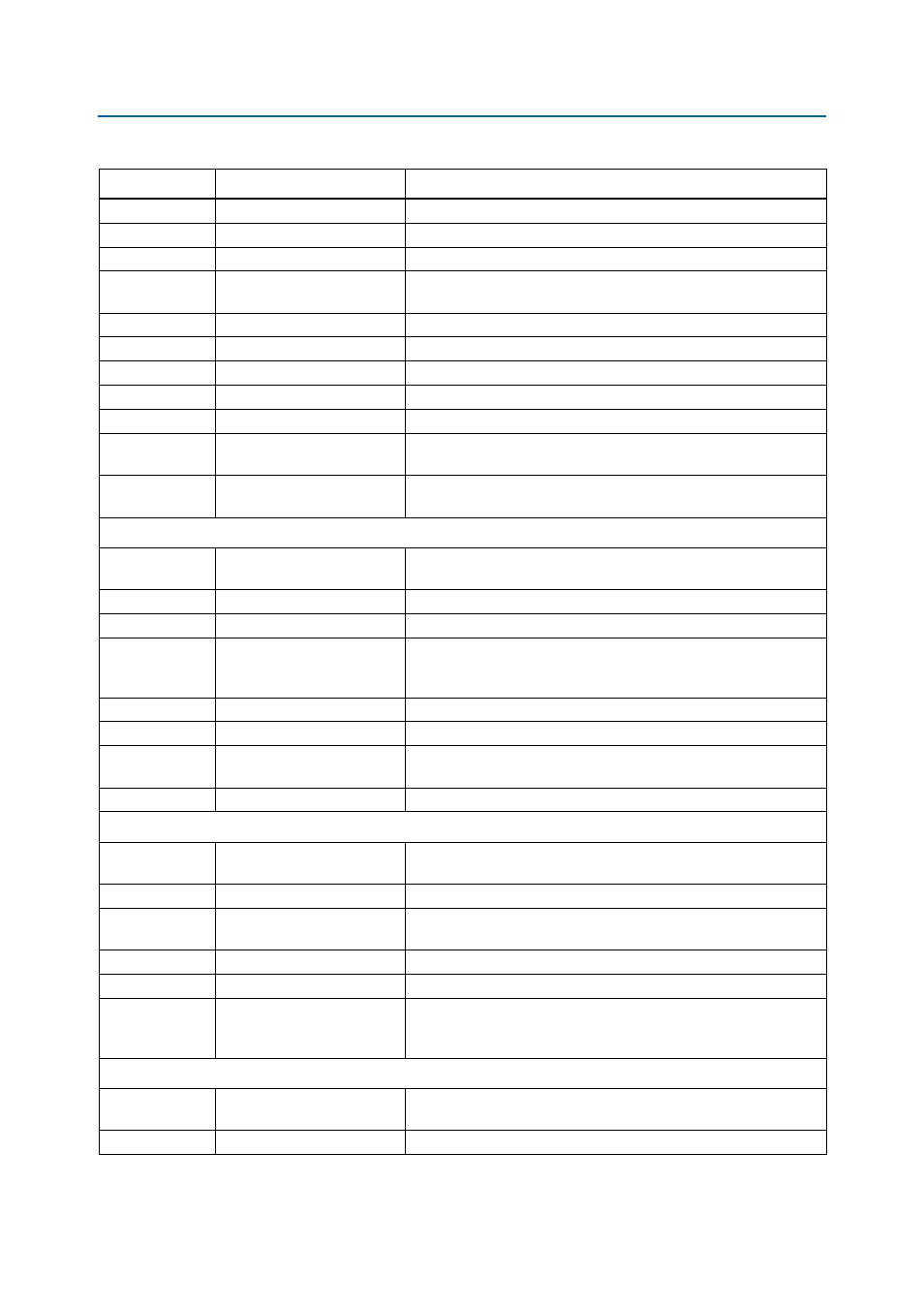
D26
Load LED
Illuminates during embedded USB-Blaster data transfers.
D27
Error LED
Illuminates when the FPGA configuration from flash fails.
D24
Power LED
Illuminates when 12-V power is present.
D32, D33, D34,
D35
Ethernet LEDs
Shows the connection speed as well as transmit or receive activity.
D3, D4
HSMC port A LEDs
You can configure these LEDs to indicate transmit or receive activity.
D1
HSMC port A Present LED
Illuminates when a daughtercard is plugged into the HSMC port A.
D14, D15
HSMC port B LEDs
You can configure these LEDs to indicate transmit or receive activity.
D2
HSMC port B Present LED
Illuminates when a daughtercard is plugged into the HSMC port B.
D30
SDI mute LED
Illuminates when the SDI receiver is muted.
D25
PCI Express Gen 2 LED
You can configure this LED to illuminate when PCI Express is in Gen 2
mode.
D37, D38, D39
PCI Express Link LEDs
You can configure these LEDs to display the PCI Express link width
(x1, x4, x8).
Clock Circuitry
X1
125 M oscillator
125.000-MHz crystal oscillator for Gigabit Ethernet, Serial RapidIO™
(SRIO), or PCI Express.
X2
156 M oscillator
156.250-MHz crystal oscillator for 10 Gigabit Ethernet or XAUI.
X3
148 M oscillator
148.500-MHz voltage controlled crystal oscillator for SDI Video.
X6
100 M oscillator
100.000-MHz crystal oscillator for PCI Express or general use such as
memories. Multiplex with CLKIN_SMA_P based on CLK_SEL switch
value.
X7
155 M oscillator
155.520-MHz crystal oscillator for SONET.
X8
50 M oscillator
50.000-MHz crystal oscillator for general purpose logic.
J15, J14
Clock input SMAs
Drives LVPECL-compatible clock inputs into the U50 clock multiplexer
buffer.
J9
Clock output SMA
Drives out 2.5-V CMOS clock outputs from the FPGA.
General User Input and Output
D6-D13
D16-D23
User LEDs
16 user LEDs. Illuminates when driven low.
SW3
User DIP switch
Octal user DIP switches. When the switch is ON, a logic 0 is selected.
S1
Reset configuration push
button
Reconfigures the FPGA from the flash memory.
S2
CPU reset push button
Resets the Max II CPLD EPM2210 System Controller and FPGA logic.
S3, S4, S5
General user push buttons
Three user push buttons. Driven low when pressed.
SW2
Power monitor rotary switch
Selects the power rail being measured and also the FPGA image to load
on power-up; 0 selects factory image and 1 selects user-defined
image.
Memory Devices
U5, U12, U18,
U24
DDR3 x64 bottom port
A single 64-bit 512-MB memory port.
U14
DDR3 x16 top port
Independent 16-bit 128-MB memory port.
Table 2–1. Stratix IV GX FPGA Development Board Components (Part 2 of 3)
Board Reference
Type
Description