Altera Stratix IV GX FPGA Development Board User Manual
Page 51
Chapter 2: Board Components
2–43
Components and Interfaces
August 2012
Altera Corporation
Stratix IV GX FPGA Development Board
Reference Manual
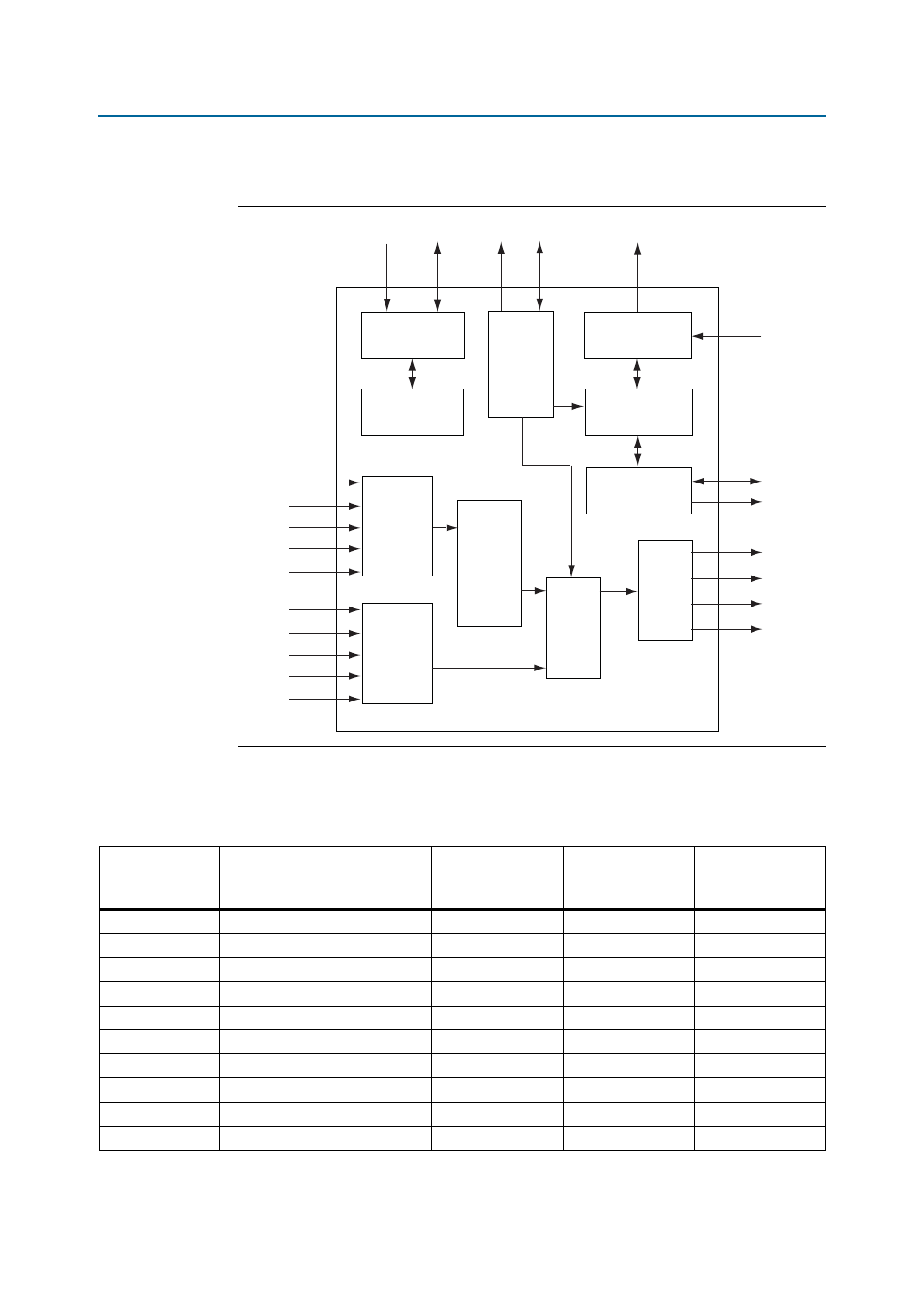
shows a block diagram of the AD9889B HDMI transmitter device.
lists the HDMI video output interface pin assignments, signal names, and
functions.
Figure 2–12. AD9889B HDMI Transmitter Device Block Diagram
Video
Data
Capture
Audio
Data
Capture
Color
Space
Conversion
4:2:2 to 4:4:4
Conversion
XOR
Mask
HDMI
Tx
Core
HDCP
Core
I
2
C Slave
Register Configuration
Logic
I
2
C Master
HDCP-EDID
Microcontroller
Interrupt
Handler
AD9889B
SCL
SDA
MCL
MDA
INT
HPD
DDCSDA
DDCSCL
Tx0– /Tx0+
Tx1– / Tx1+
Tx2– / Tx2+
TxC– / TxC+
SCLK
LRCLK
MCLK
S/PDIF
D [23:0]
DE
HSYNC
VSYNC
CLK
I
2
S [3:0]
Table 2–40. HDMI Video Output Pin Assignments, Schematic Signal Names, and Functions (Part 1 of 2)
Board Reference
Description
Schematic Signal
Name
I/O Standard
Stratix IV GX
Device
Pin Number
U25.B1
Video data bus
HDMI_D0
1.8-V
AW34
U25.A1
Video data bus
HDMI_D1
1.8-V
AL25
U25.B2
Video data bus
HDMI_D2
1.8-V
AK25
U25.A2
Video data bus
HDMI_D3
1.8-V
AP26
U25.B3
Video data bus
HDMI_D4
1.8-V
AH26
U25.A3
Video data bus
HDMI_D5
1.8-V
AM26
U25.B4
Video data bus
HDMI_D6
1.8-V
AK26
U25.A4
Video data bus
HDMI_D7
1.8-V
AN26
U25.B5
Video data bus
HDMI_D8
1.8-V
AP27
U25.A5
Video data bus
HDMI_D9
1.8-V
AN27