Qdrii+ top port 0, Qdrii+ top port 0 –53 – Altera Stratix IV GX FPGA Development Board User Manual
Page 61
Chapter 2: Board Components
2–53
Memory
August 2012
Altera Corporation
Stratix IV GX FPGA Development Board
Reference Manual
lists the DDR3 component reference and manufacturing information.
QDRII+ Top Port 0
The QDRII+ top port 0 consists of a single QDRII+ burst-of-4 SRAM, providing
4 Mbyte with an 18-bit read data bus and an 18-bit write data bus.
This memory interface is designed to run between 120 MHz, the minimum frequency
for this device, and 400 MHz for a maximum theoretical bandwidth of over 14.4 Gbps
for reading and 14.4 Gbps for writing. The internal bus in the FPGA is typically 2 or 4
times the width at full rate or half rate respectively. For example, a 400 MHz 18-bit
interface becomes a 200 MHz 72 bit bus.
lists the QDRII+ top port 0
pin assignments, signal names, and functions.
The signal names and types are relative to the Stratix IV GX device in terms of I/O
setting and direction.
U14.C2
Data bus byte lane 1
DDR3TOP_DQ11
1.5-V SSTL Class I
E22
U14.A7
Data bus byte lane 1
DDR3TOP_DQ12
1.5-V SSTL Class I
G22
U14.A2
Data bus byte lane 1
DDR3TOP_DQ13
1.5-V SSTL Class I
F23
U14.B8
Data bus byte lane 1
DDR3TOP_DQ14
1.5-V SSTL Class I
H22
U14.A3
Data bus byte lane 1
DDR3TOP_DQ15
1.5-V SSTL Class I
D23
U14.D3
Write mask byte lane 1
DDR3TOP_DM1
1.5-V SSTL Class I
G23
U14.C7
Data strobe P byte lane 1
DDR3TOP_DQS_P1
1.5-V SSTL Class I
J23
U14.B7
Data strobe N byte lane 1
DDR3TOP_DQS_N1
1.5-V SSTL Class I
H23
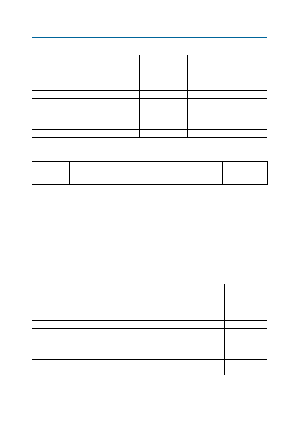
Table 2–48. DDR3 Top Port Pin Assignments, Signal Names and Functions (Part 3 of 3)
Board Reference
Description
Schematic Signal
Name
I/O Standard
Stratix IV GX
Device
Pin Number
Table 2–49. DDR3 Component Reference and Manufacturing Information
Board Reference
Description
Manufacturer
Manufacturing
Part Number
Manufacturer
Website
U14
8 M × 16-bit × 8 banks, 667M, CL9
Micron
MT41J64M16LA-15E
Table 2–50. QDRII+ Top Port 0 Pin Assignments, Signal Names and Functions (Part 1 of 3)
Board Reference
Description
Schematic Signal Name
I/O Standard
Stratix IV GX
Device
Pin Number
U22.A10
Address bus
QDR2TOP0_A19
1.5-V HSTL Class I
A28
U22.A3
Address bus
QDR2TOP0_A18
1.5-V HSTL Class I
J24
U22.A9
Address bus
QDR2TOP0_A17
1.5-V HSTL Class I
C28
U22.R7
Address bus
QDR2TOP0_A16
1.5-V HSTL Class I
G28
U22.R5
Address bus
QDR2TOP0_A15
1.5-V HSTL Class I
C30
U22.R4
Address bus
QDR2TOP0_A14
1.5-V HSTL Class I
C29
U22.R3
Address bus
QDR2TOP0_A13
1.5-V HSTL Class I
B28
U22.P8
Address bus
QDR2TOP0_A12
1.5-V HSTL Class I
R24
U22.P7
Address bus
QDR2TOP0_A11
1.5-V HSTL Class I
N20