Altera Stratix IV GX FPGA Development Board User Manual
Page 62
2–54
Chapter 2: Board Components
Memory
Stratix IV GX FPGA Development Board
August 2012
Altera Corporation
Reference Manual
U22.P5
Address bus
QDR2TOP0_A10
1.5-V HSTL Class I
A31
U22.P4
Address bus
QDR2TOP0_A9
1.5-V HSTL Class I
A29
U22.N7
Address bus
QDR2TOP0_A8
1.5-V HSTL Class I
P20
U22.N6
Address bus
QDR2TOP0_A7
1.5-V HSTL Class I
B31
U22.N5
Address bus
QDR2TOP0_A6
1.5-V HSTL Class I
B29
U22.C7
Address bus
QDR2TOP0_A5
1.5-V HSTL Class I
D27
U22.C5
Address bus
QDR2TOP0_A4
1.5-V HSTL Class I
F26
U22.B8
Address bus
QDR2TOP0_A3
1.5-V HSTL Class I
A27
U22.B4
Address bus
QDR2TOP0_A2
1.5-V HSTL Class I
G26
U22.R8
Address bus
QDR2TOP0_A1
1.5-V HSTL Class I
P24
U22.R9
Address bus
QDR2TOP0_A0
1.5-V HSTL Class I
N21
U22.N2
Write data bus
QDR2TOP0_D17
1.5-V HSTL Class I
B25
U22.M3
Write data bus
QDR2TOP0_D16
1.5-V HSTL Class I
G24
U22.L3
Write data bus
QDR2TOP0_D15
1.5-V HSTL Class I
F24
U22.J3
Write data bus
QDR2TOP0_D14
1.5-V HSTL Class I
M24
U22.G2
Write data bus
QDR2TOP0_D13
1.5-V HSTL Class I
K23
U22.F3
Write data bus
QDR2TOP0_D12
1.5-V HSTL Class I
M23
U22.D2
Write data bus
QDR2TOP0_D11
1.5-V HSTL Class I
R22
U22.C3
Write data bus
QDR2TOP0_D10
1.5-V HSTL Class I
N22
U22.B3
Write data bus
QDR2TOP0_D9
1.5-V HSTL Class I
P22
U22.C11
Write data bus
QDR2TOP0_D8
1.5-V HSTL Class I
A26
U22.D11
Write data bus
QDR2TOP0_D7
1.5-V HSTL Class I
B26
U22.E10
Write data bus
QDR2TOP0_D6
1.5-V HSTL Class I
C25
U22.G11
Write data bus
QDR2TOP0_D5
1.5-V HSTL Class I
C26
U22.J11
Write data bus
QDR2TOP0_D4
1.5-V HSTL Class I
D25
U22.K10
Write data bus
QDR2TOP0_D3
1.5-V HSTL Class I
D26
U22.M11
Write data bus
QDR2TOP0_D2
1.5-V HSTL Class I
E25
U22.N11
Write data bus
QDR2TOP0_D1
1.5-V HSTL Class I
G25
U22.P10
Write data bus
QDR2TOP0_D0
1.5-V HSTL Class I
F25
U22.B6
Write clock P
QDR2TOP0_K_P
1.5-V HSTL Class I
P23
U22.A6
Write clock N
QDR2TOP0_K_N
1.5-V HSTL Class I
N23
U22.A4
Write port select
QDR2TOP0_WPSn
1.5-V HSTL Class I
K24
U22.B7
Write byte write select 0
QDR2TOP0_BWSn0
1.5-V HSTL Class I
L23
U22.A5
Write byte write select 1
QDR2TOP0_BWSn1
1.5-V HSTL Class I
J25
U22.R6
Termination enable
QDR2TOP0_ODT
1.5-V HSTL Class I
A22
U22.P3
Read data bus
QDR2TOP0_Q17
1.5-V HSTL Class I
M25
U22.N3
Read data bus
QDR2TOP0_Q16
1.5-V HSTL Class I
L25
U22.L2
Read data bus
QDR2TOP0_Q15
1.5-V HSTL Class I
N25
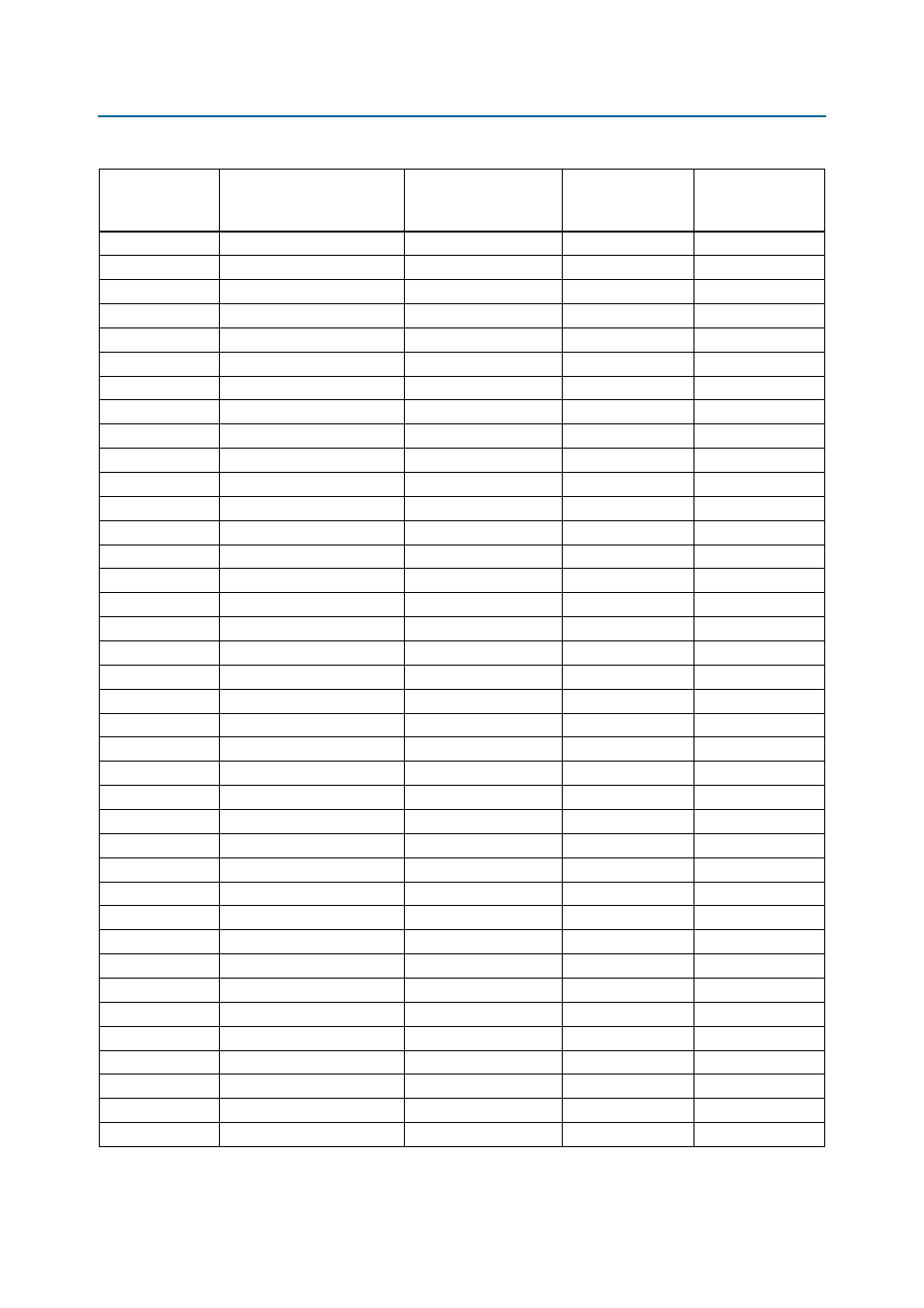
Table 2–50. QDRII+ Top Port 0 Pin Assignments, Signal Names and Functions (Part 2 of 3)
Board Reference
Description
Schematic Signal Name
I/O Standard
Stratix IV GX
Device
Pin Number