Board overview, Board overview –2, Figure 2–1 – Altera Stratix IV GX FPGA Development Board User Manual
Page 10: Table 2–1
2–2
Chapter 2: Board Components
Board Overview
Stratix IV GX FPGA Development Board
August 2012
Altera Corporation
Reference Manual
Board Overview
This section provides an overview of the Stratix IV GX FPGA development board,
including an annotated board image and component descriptions.
provides an overview of the development board features.
describes the components and lists their corresponding board references.
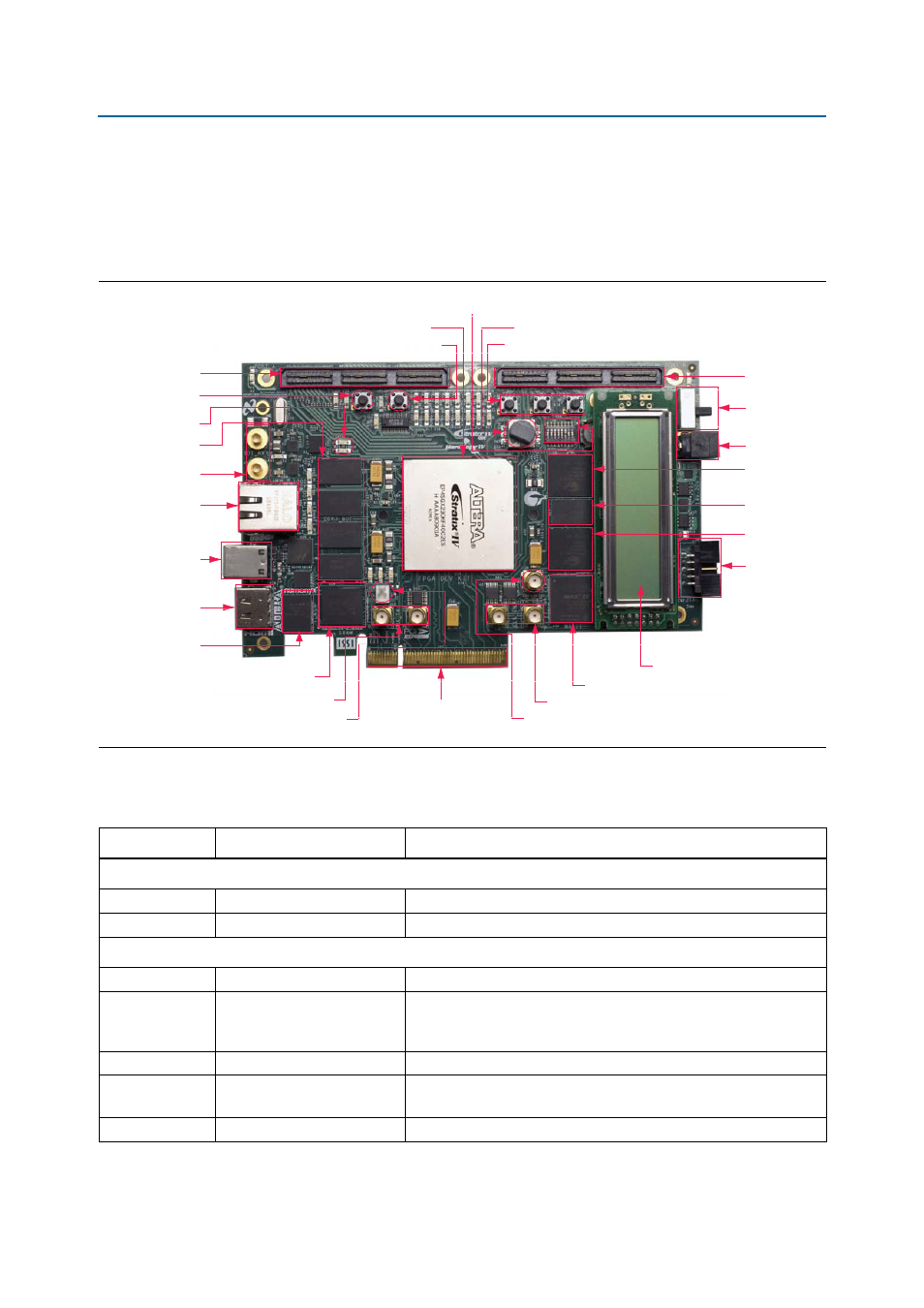
Figure 2–1. Overview of the Stratix IV GX FPGA Development Board Features
Flash x16 Memory
(U32)
Configuration Done
LED (D5)
SSRAM x36 Memory (U30)
Clock Input SMA Connector (J14, J15)
CPU Reset Push-button Switch (S2)
Clock Output SMA Connector (J9)
Max II CPLD EPM2210 System Controller (U31)
Character LCD (J16)
Stratix IV GX FPGA (U13)
HSMC Port B
(J2)
HSMC Port A (J1)
Fan Power Header
Transceiver TX SMA Connectors
SDI Video Port
(J3, J5)
Gigabit Ethernet Port
(J6)
USB Type-B
Connector (J7)
HDMI Video Port (J11)
Reset Configuration
Push-Button
Switch (S1)
DDR3 x64 Bottom Port
(U5, U12, U18, U24)
General User Push-button Switches (S3, S4, S5)
Power Monitor Rotary Switch (SW2)
Power Switch
(SW1)
User DIP Switch (SW3)
DC Input Jack (J4)
QDRII+ x18/x18
Top Port 1 (U7)
DDR3 x16
Top Port (U14)
QDRII+ x18/x18
Top Port 0 (U22)
JTAG Connector
(J8)
PCI Express Edge Connector
(J17)
Table 2–1. Stratix IV GX FPGA Development Board Components (Part 1 of 3)
Board Reference
Type
Description
Featured Devices
U13
FPGA
EP4SGX230KF40, 1517-pin BGA.
U31
CPLD
EPM2210GF256, 256-pin BGA.
Configuration, Status, and Setup Elements
SW6
JTAG DIP switch
Enables and disables devices in the JTAG chain.
SW4
Board Settings DIP switch
Controls the Max
II CPLD EPM2210 System Controller functions such
as clock enable, power and temperature monitor, as well as voltage
settings for transceivers and SMA clock input control.
J8
JTAG connector
Disables embedded blaster (for use with external USB-Blasters).
SW5
PCI Express DIP switch
Controls the PCI Express lane width by connecting prsnt pins
together on the PCI Express edge connector.
D5
Configuration done LED
Illuminates when the FPGA is configured.