Ddr3 top port, Ddr3 top port –51 – Altera Stratix IV GX FPGA Development Board User Manual
Page 59
Chapter 2: Board Components
2–51
Memory
August 2012
Altera Corporation
Stratix IV GX FPGA Development Board
Reference Manual
lists the DDR3 component reference and manufacturing information.
DDR3 Top Port
The DDR3 top port consists of a single DDR3 devices, providing 128 Mbyte with a
16-bit data bus. The board supports addressing for up to 4 times the memory if larger
devices become available.
This memory interface is designed to run between 300 MHz, the minimum frequency
for DDR3, and 533 MHz for a maximum theoretical bandwidth of over 68.2 Gbps. The
internal bus in the FPGA is typically 2 or 4 times the width at full rate or half rate
respectively. For example, a 533 MHz 64-bit interface will become a 267 MHz 256-bit
bus.
lists the DDR3 top port pin assignments, signal names, and its functions.
The signal names and types are relative to the Stratix IV device in terms of I/O setting
and direction.
U24.F3
Data strobe P byte lane 6
DDR3BOT_DQS_P6
1.5-V SSTL Class I
AT26
U24.G3
Data strobe N byte lane 6
DDR3BOT_DQS_N6
1.5-V SSTL Class I
AU26
U24.D7
Data bus byte lane 7
DDR3BOT_DQ56
1.5-V SSTL Class I
AJ23
U24.C3
Data bus byte lane 7
DDR3BOT_DQ57
1.5-V SSTL Class I
AK24
U24.C8
Data bus byte lane 7
DDR3BOT_DQ58
1.5-V SSTL Class I
AF23
U24.C2
Data bus byte lane 7
DDR3BOT_DQ59
1.5-V SSTL Class I
AH23
U24.A7
Data bus byte lane 7
DDR3BOT_DQ60
1.5-V SSTL Class I
AG22
U24.A2
Data bus byte lane 7
DDR3BOT_DQ61
1.5-V SSTL Class I
AJ22
U24.B8
Data bus byte lane 7
DDR3BOT_DQ62
1.5-V SSTL Class I
AH22
U24.A3
Data bus byte lane 7
DDR3BOT_DQ63
1.5-V SSTL Class I
AE22
U24.D3
Write mask byte lane 7
DDR3BOT_DM7
1.5-V SSTL Class I
AF22
U24.C7
Data strobe P byte lane 7
DDR3BOT_DQS_P7
1.5-V SSTL Class I
AK23
U24.B7
Data strobe N byte lane 7
DDR3BOT_DQS_N7
1.5-V SSTL Class I
AL23
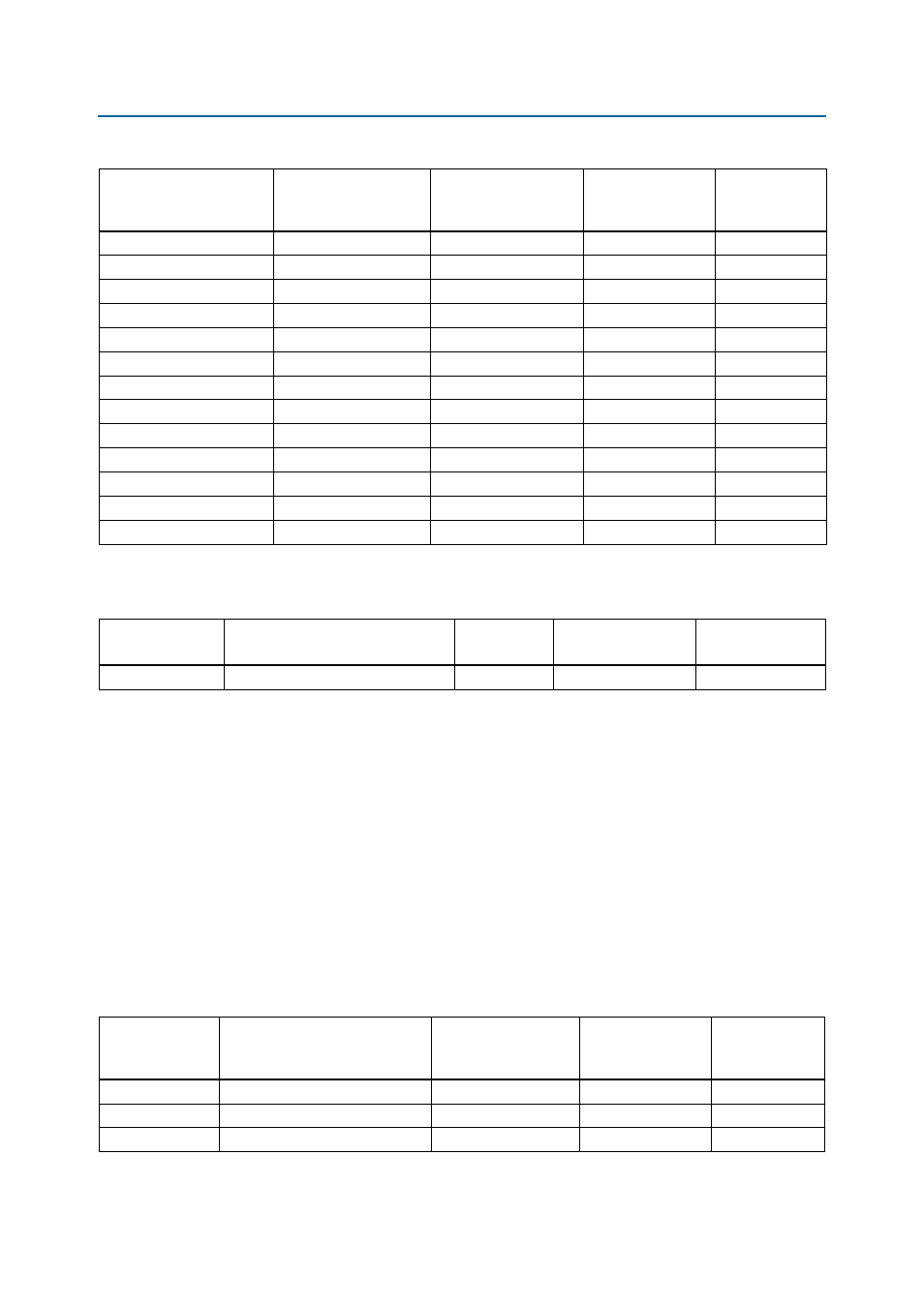
Table 2–46. DDR3 Bottom Port Pin Assignments, Schematic Signal Names, and Functions (Part 4 of 4)
Board Reference
Description
Schematic Signal
Name
I/O Standard
Stratix IV GX
Device
Pin Number
Table 2–47. DDR3 Component Reference and Manufacturing Information
Board Reference
Description
Manufacturer
Manufacturing
Part Number
Manufacturer
Website
U5, U12, U18, U24
8 M × 16-bit × 8 banks, 667M, CL9
Micron
MT41J64M16LA-15E
Table 2–48. DDR3 Top Port Pin Assignments, Signal Names and Functions (Part 1 of 3)
Board Reference
Description
Schematic Signal
Name
I/O Standard
Stratix IV GX
Device
Pin Number
U14.T7
Address bus
DDR3TOP_A14
1.5-V SSTL Class I
B20
U14.T3
Address bus
DDR3TOP_A13
1.5-V SSTL Class I
M22
U14.N7
Address bus
DDR3TOP_A12
1.5-V SSTL Class I
A23