Ddr3 bottom port, Ddr3 bottom port –48 – Altera Stratix IV GX FPGA Development Board User Manual
Page 56
2–48
Chapter 2: Board Components
Memory
Stratix IV GX FPGA Development Board
August 2012
Altera Corporation
Reference Manual
DDR3 Bottom Port
The DDR3 bottom port consists of four DDR3 devices, providing a single 512-Mbyte
interface with a 64-bit data bus. The board supports addressing for up to 4 times the
memory if larger devices become available.
This memory interface is designed to run between 300 MHz, the minimum frequency
for DDR3, and 533 MHz for a maximum theoretical bandwidth of over 68.2 Gbps. The
internal bus in the FPGA is typically 2 or 4 times the width at full-rate or half-rate
respectively. For example, a 533 MHz 64-bit interface will become a 267 MHz 256-bit
bus.
lists the DDR3 DIMM
pin assignments, signal names, and functions. The
signal names and types are relative to the Stratix IV device in terms of I/O setting and
direction.
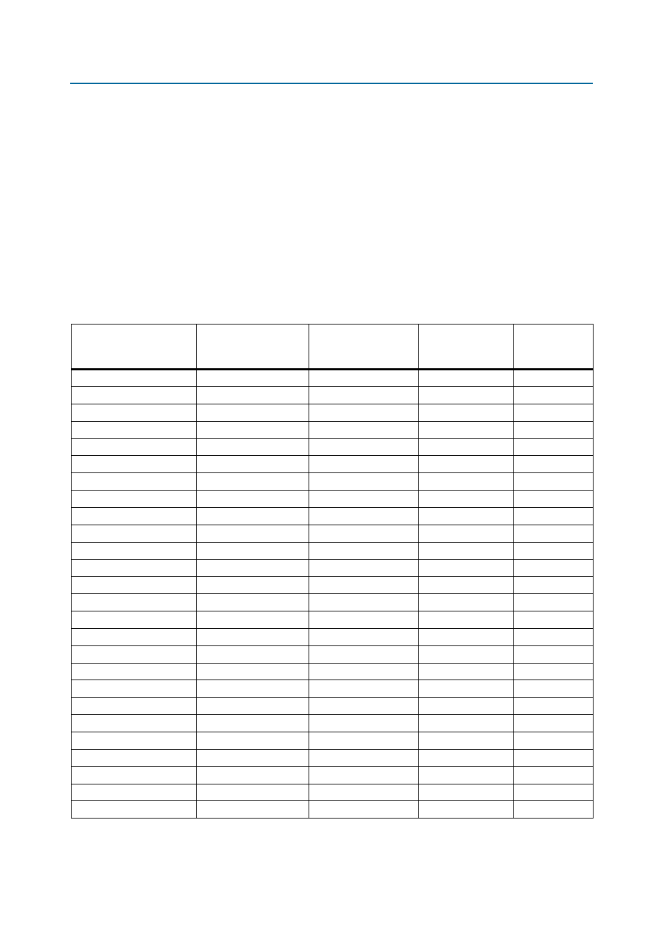
Table 2–46. DDR3 Bottom Port Pin Assignments, Schematic Signal Names, and Functions (Part 1 of 4)
Board Reference
Description
Schematic Signal
Name
I/O Standard
Stratix IV GX
Device
Pin Number
U5, U12, U18, U24 pin T7
Address bus
DDR3BOT_A14
1.5-V SSTL Class I
AJ14
U5, U12, U18, U24 pin T3
Address bus
DDR3BOT_A13
1.5-V SSTL Class I
AN15
U5, U12, U18, U24 pin N7
Address bus
DDR3BOT_A12
1.5-V SSTL Class I
AE14
U5, U12, U18, U24 pin R7
Address bus
DDR3BOT_A11
1.5-V SSTL Class I
AJ13
U5, U12, U18, U24 pin L7
Address bus
DDR3BOT_A10
1.5-V SSTL Class I
AE16
U5, U12, U18, U24 pin R3
Address bus
DDR3BOT_A9
1.5-V SSTL Class I
AK14
U5, U12, U18, U24 pin T8
Address bus
DDR3BOT_A8
1.5-V SSTL Class I
AH13
U5, U12, U18, U24 pin R2
Address bus
DDR3BOT_A7
1.5-V SSTL Class I
AP15
U5, U12, U18, U24 pin R8
Address bus
DDR3BOT_A6
1.5-V SSTL Class I
AG14
U5, U12, U18, U24 pin P2
Address bus
DDR3BOT_A5
1.5-V SSTL Class I
AL15
U5, U12, U18, U24 pin P8
Address bus
DDR3BOT_A4
1.5-V SSTL Class I
AF16
U5, U12, U18, U24 pin N2
Address bus
DDR3BOT_A3
1.5-V SSTL Class I
AT14
U5, U12, U18, U24 pin P3
Address bus
DDR3BOT_A2
1.5-V SSTL Class I
AH14
U5, U12, U18, U24 pin P7
Address bus
DDR3BOT_A1
1.5-V SSTL Class I
AG15
U5, U12, U18, U24 pin N3
Address bus
DDR3BOT_A0
1.5-V SSTL Class I
AK13
U5, U12, U18, U24 pin M3
Bank address bus
DDR3BOT_BA2
1.5-V SSTL Class I
AE15
U5, U12, U18, U24 pin M3
Bank address bus
DDR3BOT_BA1
1.5-V SSTL Class I
AD15
U5, U12, U18, U24 pin M3
Bank address bus
DDR3BOT_BA0
1.5-V SSTL Class I
AF14
U5, U12, U18, U24 pin J3
Row address select
DDR3BOT_RASn
1.5-V SSTL Class I
AW21
U5, U12, U18, U24 pin T2
Reset
DDR3BOT_RSTn
1.5-V SSTL Class I
AP20
U5, U12, U18, U24 pin K3
Column address select
DDR3BOT_CASn
1.5-V SSTL Class I
AV19
U5, U12, U18, U24 pin L2
Chip select
DDR3BOT_CSn
1.5-V SSTL Class I
AN20
U5, U12, U18, U24 pin L3
Write enable
DDR3BOT_WEn
1.5-V SSTL Class I
AW20
U5, U12, U18, U24 pin K1
Termination enable
DDR3BOT_ODT
1.5-V SSTL Class I
AU20
U5, U12, U18, U24 pin K9
Clock enable
DDR3BOT_CKE
1.5-V SSTL Class I
AW19
U5, U12, U18, U24 pin J7
Clock P
DDR3BOT_CK_P
1.5-V SSTL Class I
AE20