Development board block diagram, Handling the board, General user i/o – Altera Arria V GT FPGA Development Board User Manual
Page 9: Leds and displays, Eight dual color user leds, Two hsmc interface transmit/receive (tx/rx) leds, Push buttons, One cpu reset push button, Three general user push buttons, Eight user control dip switches
Chapter 1: Overview
1–5
Development Board Block Diagram
December 2014
Altera Corporation
Arria V GT FPGA Development Board
Reference Manual
■
General user I/O
■
LEDs and displays
■
Eight dual color user LEDs
■
Two HSMC interface transmit/receive (TX/RX) LEDs
■
Push buttons
■
One CPU reset push button
■
Three general user push buttons
■
Eight user control DIP switches
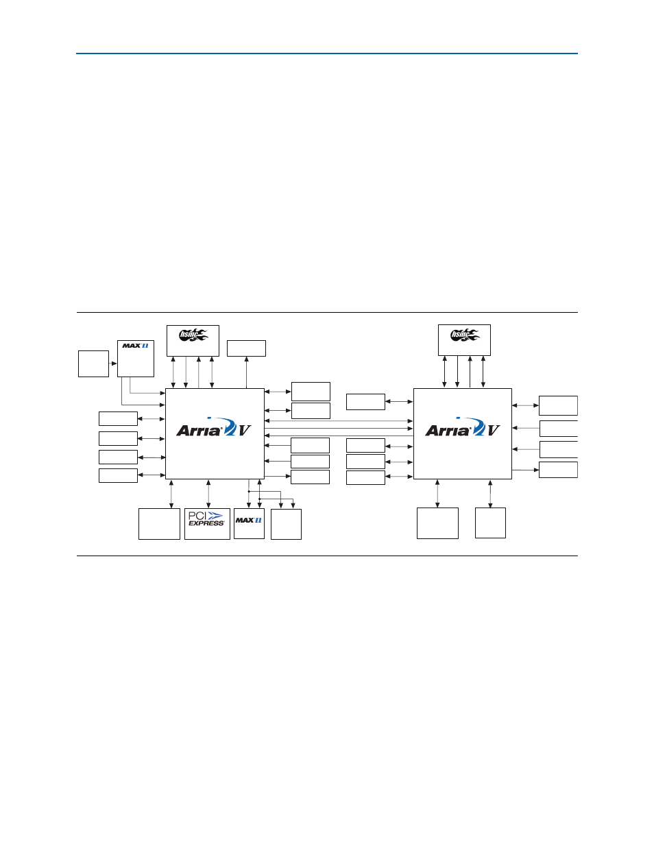
Development Board Block Diagram
shows a block diagram of the Arria V GT FPGA development board.
Handling the Board
When handling the board, it is important to observe the following static discharge
precaution:
c
Without proper anti-static handling, the board can be damaged. Therefore, use
anti-static handling precautions when touching the board.
Figure 1–1. Arria V GT FPGA Development Board Block Diagram
Port B
Port A
1152-MB
DDR3
2x16 LCD
Push buttons
8 bi-color LEDs
CPLD
1-Gb
Flash
FMC
x8 Edge
SMAs
10G
Gigabit Ethernet
PHY (RGMII)
On-Board
USB-Blaster II
and
USB Interface
Mini-USB
2.0
XCVR x1
Bull’s Eye
10G
XCVR x3
SDI
TX/RX
XCVR x1
Bull’s Eye
10G
Bull’s Eye
6G
XCVR x1
XCVR x1
SMAs
10G
XCVR x1
SFP+
XCVR x2
x16
x72
DDR3
(x64)
x32 Hard IP
(x64 Soft IP)
72-Mb
QDRII+
x36
x11
x8
x4
ADDR x16
XCVR x8 Chip-to Chip
LVDS x29 Chip-to Chip + 1 Clock Input
LVDS x29 Chip-to Chip + 1 Clock Input
XVCR x8
XVCR x10
x80
CLKIN x3
CLKOUT x3
XCVR x4
x80
CLKIN x3
CLKOUT x3
XCVR x8
JTAG Chain
USB Interface x19
Programmable
Oscillators +
50 M, 100 M
Programmable
Oscillators +
50 M, 100 M
5AGTFD7K3F40
FPGA 1
5AGTFD7K3F40
FPGA 2
x16
Push Buttons
DIP Switches
DIP Switches
8 bi-color LEDs
x8
x4
x16