User-defined leds, General user-defined leds, User-defined leds –28 – Altera Arria V GT FPGA Development Board User Manual
Page 38: General user-defined leds –28
2–28
Chapter 2: Board Components
General User Input/Output
Arria V GT FPGA Development Board
December 2014
Altera Corporation
Reference Manual
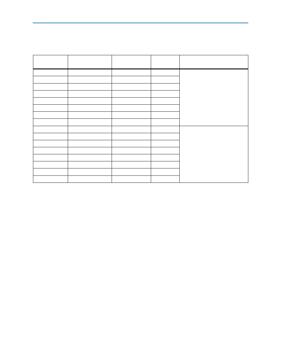
Table 2–15
lists the user-defined DIP switch schematic signal names and their
corresponding Arria V GT FPGA pin numbers.
User-Defined LEDs
The development board includes general and user-defined LEDs. This section
describes all user-defined LEDs. For information on board specific or status LEDs,
refer to
“Status Elements” on page 2–18
General User-Defined LEDs
Board references D18 through D25 and D26 through D33 are two sets of eight pairs
user-defined LEDs. Each of the Arria V GT FPGA have a set of user-defined LEDs.
The LEDs illuminate when a logic 0 is driven, and turns off when a logic 1 is driven.
There are no board-specific functions for these LEDs.
Table 2–15. User-defined DIP Switch Schematic Signal Names and Functions
Board Reference
Schematic
Signal Name
Arria V GT FPGA
Pin Number
I/O Standard
Description
SW2.1
USER1_DIPSW0
P18
2.5-V
User-defined DIP switch that
connects to FPGA 1.
SW2.2
USER1_DIPSW1
N18
2.5-V
SW2.3
USER1_DIPSW2
C16
2.5-V
SW2.4
USER1_DIPSW3
B16
2.5-V
SW2.5
USER1_DIPSW4
G17
2.5-V
SW2.6
USER1_DIPSW5
F17
2.5-V
SW2.7
USER1_DIPSW6
D17
2.5-V
SW2.8
USER1_DIPSW7
C17
2.5-V
SW3.1
USER2_DIPSW0
C8
2.5-V
User-defined DIP switch that
connects to FPGA 2.
SW3.2
USER2_DIPSW1
D8
2.5-V
SW3.3
USER2_DIPSW2
E7
2.5-V
SW3.4
USER2_DIPSW3
E6
2.5-V
SW3.5
USER2_DIPSW4
G8
2.5-V
SW3.6
USER2_DIPSW5
F8
2.5-V
SW3.7
USER2_DIPSW6
D15
2.5-V
SW3.8
USER2_DIPSW7
G11
2.5-V