Board overview, Board overview –2, Figure 2–1 – Altera Arria V GT FPGA Development Board User Manual
Page 12: Table 2–1
2–2
Chapter 2: Board Components
Board Overview
Arria V GT FPGA Development Board
December 2014
Altera Corporation
Reference Manual
Board Overview
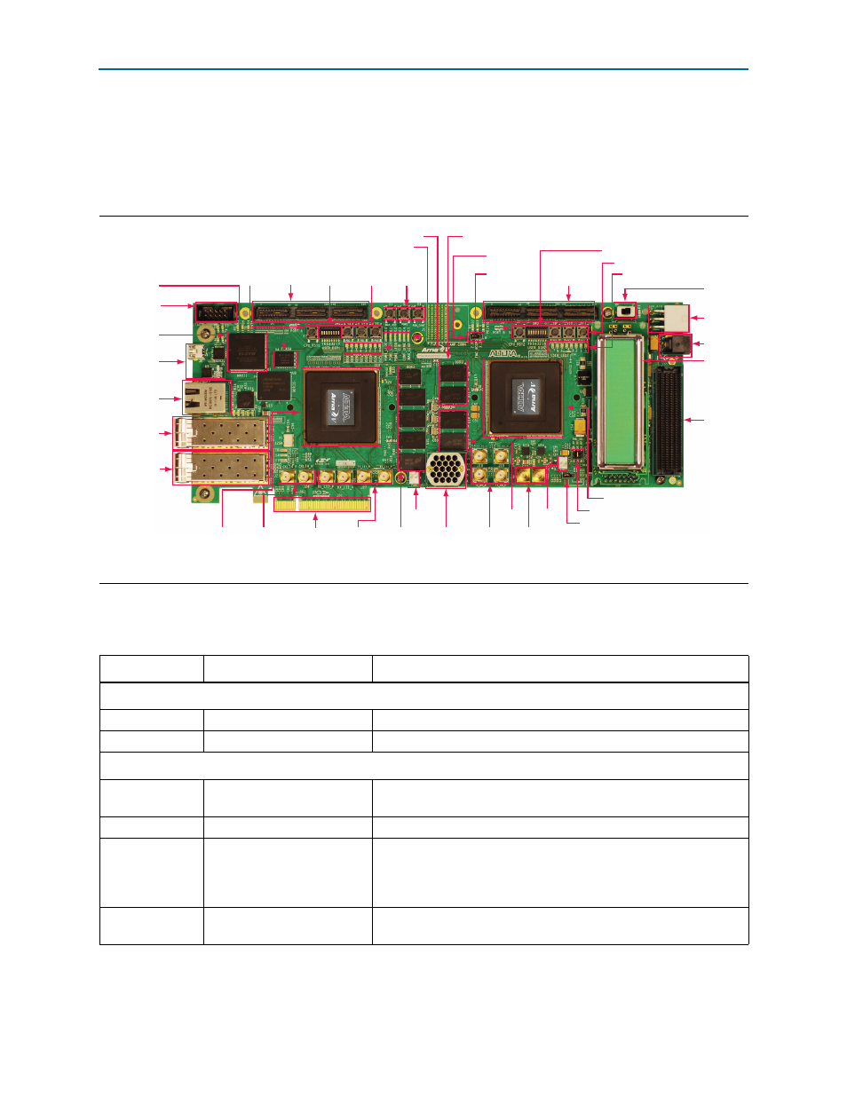
This section provides an overview of the Arria V GT FPGA development board,
including an annotated board image and component descriptions.
shows
an overview of the available components.
describes the components and lists their corresponding board references.
Figure 2–1. Overview of the Arria V GT FPGA Development Board Features
Arria V FPGA
(U16)
Arria V FPGA (U13)
FMC Bank B Voltage Select (J11)
FMC VCCPD
B4 Select (J5)
FMC Bank B Power Source Select (J28)
MAX II CPLD
EPM2210 System
Controller (U2)
PCI
Express Edge
Connector
(J14)
JTAG Connector
(J1)
Embedded
USB-Blaster
Circuitry (J7)
Gigabit Ethernet
Port (J8)
SFP+ Port (J10)
SFP+ Port (J15)
[Available in
Arria V GT
Development
Board Only]
DC Input
Jack (J6)
Character
LCD (J29)
Board
Power Switch
(SW1)
ATX Power
Connector
(J4)
FMC
Connector
(J9)
CPU Reset
Push
Button (S4)
DDR3A
(U7, U11, U18,
U21, U28)
DDR3C
(U19, U22)
DDR3B (U6, U12)
Tx/Rx
Transceivers
(J19-J22)
Tx/Rx
Transceivers
(J12, J13,
J24, J25)
Fan Power
(J23)
Fan Power
(J14)
SDI Video
Port
(J26, J27)
Bullseye
SMA
Connector
(J16)
Clock Input
SMA
Connector
(J10, J11)
Configuration LEDs (D12-D17)
Configuration
Push Buttons
(S1-S3)
Flash
Memory (U4)
User LEDs (D18-D25)
User Push
Buttons
(S5-S7)
User LEDs (D26-D33)
User Push Buttons (S9-S11)
CPU Reset
Push Button (S8)
User DIP Switch (SW3)
User DIP
Switch (SW2)
HSMC
Port A (J2)
HSMC
Port B (J3)
Table 2–1. Arria V GT FPGA Development Board Components (Part 1 of 4)
Board Reference
Type
Description
Featured Devices
U13, U16
FPGA
Two Arria V GT FPGA, 5AGTFD7K3F40I3N, 1517-pin FBGA.
U2
CPLD
MAX II CPLD, EPM2210GF324, 324-pin
BGA.
Configuration, Status, and Setup Elements
J1
JTAG connector
Disables the on-board USB-Blaster II (for use with external
USB-Blasters).
J7
On-Board USB-Blaster II
Mini-USB 2.0 connector for programming and debugging the FPGA.
SW5
Board settings DIP switch
Controls the MAX
II CPLD EPM2210 System Controller functions such
as clock enable, SMA clock input control, and which image to load
from flash memory at power-up. This switch is located on the bottom
of the board.
SW6
JTAG chain DIP switch
Enables and disables devices in the JTAG chain. This switch is located
on the bottom of the board.