Altera Arria V GT FPGA Development Board User Manual
Page 14
2–4
Chapter 2: Board Components
Board Overview
Arria V GT FPGA Development Board
December 2014
Altera Corporation
Reference Manual
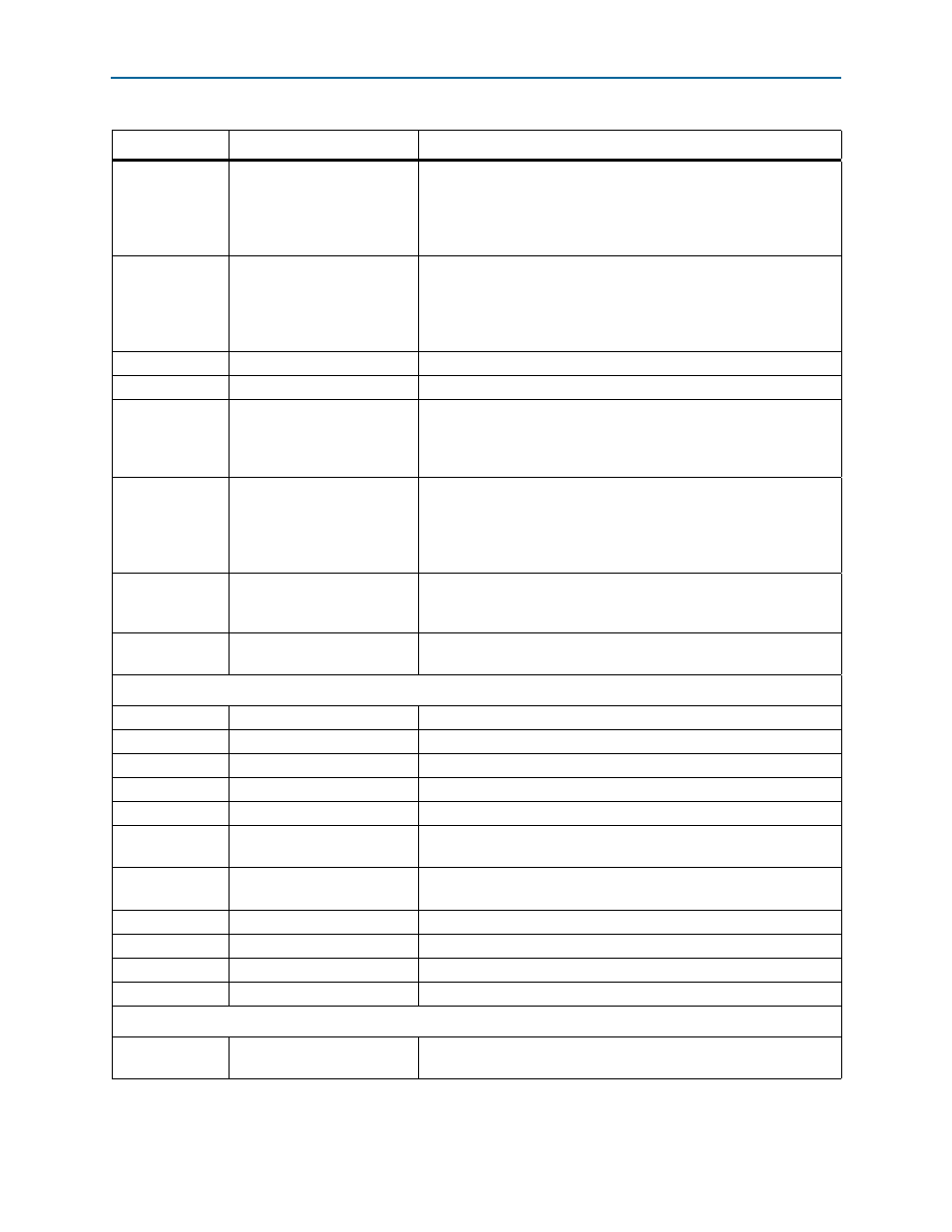
U52
Si5338 programmable
oscillator
Programmable oscillator with default frequencies of CLK0=125 MHz,
CLK1=100 MHz, CLK2=156.25 MHz, CLK3=125 MHz at I
2
C address
73 HEX. The frequency is programmable using the clock GUI with the
default MAX II CPLD EPM2210 System Controller design programmed
into the MAX II EPM2210.
U34
Si5338 programmable
oscillator
Programmable oscillator with default frequencies of CLK0=625 MHz,
CLK1=100 MHz, CLK2=625 MHz, CLK3=125 MHz at I
2
C address
72 HEX. The frequency is programmable using the clock GUI with the
default MAX II CPLD EPM2210 System Controller design programmed
into the MAX II EPM2210.
X1
125 MHz oscillator
125.000 MHz crystal oscillator for general purpose logic to FPGA 1.
X4
125 MHz oscillator
125.000 MHz crystal oscillator for general purpose logic to FPGA 2.
X2
Si571 programmable
Oscillator (148.5 MHz default)
Programmable oscillator for SDI or REFCLK0RP/N with default
frequencies at I
2
C address 55 HEX. The frequency is programmable
using the clock GUI with the default MAX II EPM2210 System
Controller design programmed into the MAX II EPM2210.
X7, or J17 and
J18 to U56 buffer
Programmable oscillator
(100 MHz default)
Programmable oscillator with a default frequency of 100.00 MHz. The
frequency is programmable using the clock GUI with the default MAX II
CPLD EPM2210 System Controller design programmed into the MAX
II EPM2210. Multiplex with CLKIN_SMA_P/N based on CLK_SEL
switch value.
X6 to U51 1:3
zero delay clock
buffer
50 MHz oscillator
50.000 MHz crystal oscillator for general purpose logic. Three outputs
connect to the FPGA 1, FPGA 2, and MAX II devices.
J17, J18
Clock input SMAs
Drive LVPECL-compatible clock inputs into the clock multiplexer buffer
(U56).
General User Input/Output
SW2
FPGA 1 user DIP switch
Octal user DIP switches. When the switch is ON, a logic 0 is selected.
SW3
FPGA 2 user DIP switch
Octal user DIP switches. When the switch is ON, a logic 0 is selected.
S1
MAX II reset push button
Resets the MAX II CPLD EPM2210 System Controller.
S4
FPGA 1 CPU reset push button Resets the FPGA 1 logic.
S8
FPGA 2 CPU reset push button Resets the FPGA 2 logic.
S5–S7
FPGA 1 general user push
buttons
Three user push buttons. Driven low when pressed.
S9–S11
FPGA 2 general user push
buttons
Three user push buttons. Driven low when pressed.
D18–D25
FPGA 1 user LEDs
Eight bi-color user LEDs. Illuminates when driven low.
D26–D33
FPGA 2 user LEDs
Eight bi-color user LEDs. Illuminates when driven low.
D35
FPGA 1 LED
LED indicator for FPGA 1.
D32
FPGA 2 LED
LED indicator for FPGA 2.
Memory Devices
U4
Flash x16 memory
Synchronous burst mode flash device that provides a 16-bit 125-MB
non-volatile memory port.
Table 2–1. Arria V GT FPGA Development Board Components (Part 3 of 4)
Board Reference
Type
Description