Altera Arria V GT FPGA Development Board User Manual
Page 21
Chapter 2: Board Components
2–11
MAX II CPLD EPM2210 System Controller
December 2014
Altera Corporation
Arria V GT FPGA Development Board
Reference Manual
FMC_SDA
V2
2.5-V
FMC module data
FPGA1_CEN
L1
2.5-V
FPGA 1 chip enable
FPGA1_CEON
F11
2.5-V
FPGA 1 chip output enable
FPGA1_CONF_DONE
M4
2.5-V
FPGA 1 configuration done
FPGA1_CONFIG_D0
D1
2.5-V
FPGA configuration data
FPGA1_CONFIG_D1
D3
2.5-V
FPGA configuration data
FPGA1_CONFIG_D2
E2
2.5-V
FPGA configuration data
FPGA1_CONFIG_D3
D4
2.5-V
FPGA configuration data
FPGA1_CONFIG_D4
E1
2.5-V
FPGA configuration data
FPGA1_CONFIG_D5
E3
2.5-V
FPGA configuration data
FPGA1_CONFIG_D6
F3
2.5-V
FPGA configuration data
FPGA1_CONFIG_D7
E4
2.5-V
FPGA configuration data
FPGA1_CONFIG_D8
F2
2.5-V
FPGA configuration data
FPGA1_CONFIG_D9
E5
2.5-V
FPGA configuration data
FPGA1_CONFIG_D10
F1
2.5-V
FPGA configuration data
FPGA1_CONFIG_D11
F4
2.5-V
FPGA configuration data
FPGA1_CONFIG_D12
G3
2.5-V
FPGA configuration data
FPGA1_CONFIG_D13
F5
2.5-V
FPGA configuration data
FPGA1_CONFIG_D14
G2
2.5-V
FPGA configuration data
FPGA1_CONFIG_D15
F6
2.5-V
FPGA configuration data
FPGA1_CVP_CONFDONE
M1
2.5-V
FPGA 1 configuration via protocol done
FPGA1_MSEL0
F8
2.5-V
FPGA 1 mode select 0
FPGA1_MSEL1
A6
2.5-V
FPGA 1 mode select 1
FPGA1_MSEL2
E8
2.5-V
FPGA 1 mode select 2
FPGA1_MSEL3
B7
2.5-V
FPGA 1 mode select 3
FPGA1_MSEL4
D8
2.5-V
FPGA 1 mode select 4
FPGA1_NCONFIG
M5
2.5-V
FPGA 1 configuration active
FPGA1_NSTATUS
N1
2.5-V
FPGA 1 configuration ready
FPGA1_PR_DONE
K4
2.5-V
FPGA 1 partial reconfiguration done
FPGA1_PR_ERROR
L5
2.5-V
FPGA 1 partial reconfiguration error
FPGA1_PR_READY
L6
2.5-V
FPGA 1 partial reconfiguration ready
FPGA1_PR_REQUEST
L2
2.5-V
FPGA 1 partial reconfiguration request
FPGA2_CEN
K5
2.5-V
FPGA 2 chip enable
FPGA2_CEON
C11
2.5-V
FPGA 2 chip output enable
FPGA2_CONF_DONE
M3
2.5-V
FPGA 2 configuration done
FPGA2_CVP_CONFDONE
B18
2.5-V
FPGA 2 configuration via protocol done
FPGA2_MSEL0
U5
2.5-V
FPGA 2 mode select 0
FPGA2_MSEL1
R7
2.5-V
FPGA 2 mode select 1
FPGA2_MSEL2
V5
2.5-V
FPGA 2 mode select 2
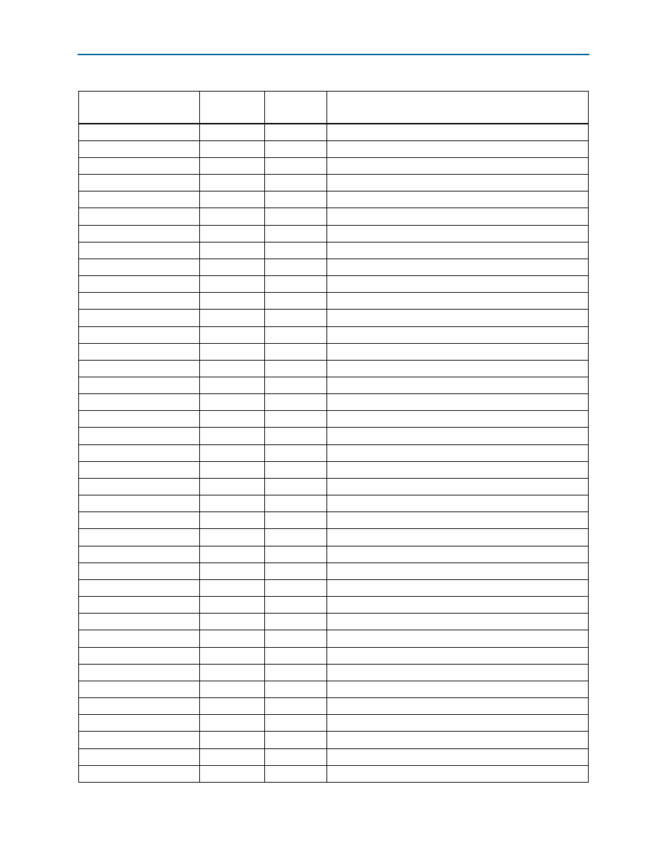
Table 2–5. MAX II CPLD EPM2210 System Controller Device Pin-Out (Part 3 of 5)
Schematic Signal Name
MAX II CPLD
Pin Number
I/O Standard
Description