Altera Arria V GT FPGA Development Board User Manual
Page 15
Chapter 2: Board Components
2–5
Board Overview
December 2014
Altera Corporation
Arria V GT FPGA Development Board
Reference Manual
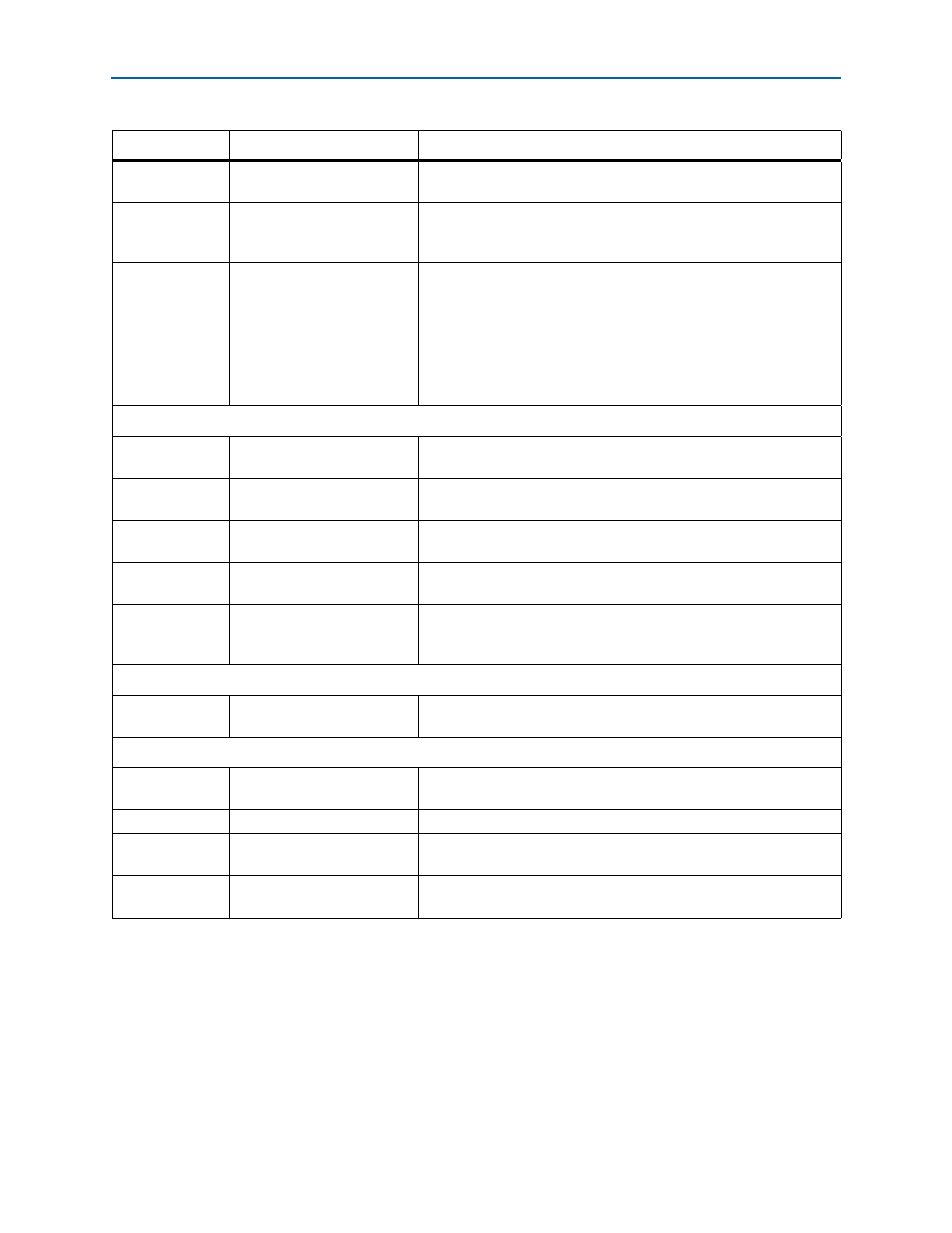
U8
QDRII+ memory
9-MB QDRII+ SRAM with a 36-bit data bus. The device has a separate
36-bit read and 36-bit write port with DDR signalling at up to 400 MHz.
U7, U11, U18,
U21, U28
DDR3A memory
DDR3 SDRAM interface on FPGA 1. This 1152-MB DDR3 x72-bit data
bus consists of four x16 devices and one x8 device with a single
address or command bus.
U6, U12, U19,
U22
DDR3B/C memory
DDR3 SDRAM interface on FPGA 2. There are two interface options:
■
Option 1: 512-MB interface with a 32-bit data bus. This DDR3
x32-bit data bus consists of two x16 devices with a single shared
address.
■
Option 2: 1024-MB interface with a 64-bit data bus. This DDR3
x64-bit data bus consists of four x16 devices with a single shared
address.
Communication Ports
J30
PCI Express edge connector
Gold-plated edge fingers connector for up to ×8 signaling in Gen1 and
x4 Gen2 modes.
J2
HSMC port A
Provides four transceiver channels and 80 CMOS or 17 LVDS channels
per the HSMC specification.
J3
HSMC port B
Provides four transceiver channels and 80 CMOS or 17 LVDS channels
per the HSMC specification.
J7
Mini-USB type-AB connector
USB interface for programming the FPGA through on-board
USB-Blaster II JTAG via a type-AB Mini-USB cable.
J8
Gigabit Ethernet
RJ-45 connector which provides a 10/100/1000 Ethernet connection
via a Marvell 88E1111 PHY and the FPGA-based Altera Triple Speed
Ethernet MegaCore function in RGMII mode.
Display Ports
J29
Character LCD connector
Connector which interfaces to the provided 16 character × 2 line LCD
module along with two standoffs at MTH7 and MTH8.
Power Supply
J6
DC input jack
Accepts a 19-V DC power supply. Do not use this input jack while the
board is plugged into a PCI Express slot.
J4
ATX power connector
PCI Express auxiliary power source option.
J30
PCI Express edge connector
Interfaces to a PCI Express root port such as an appropriate PC
motherboard.
SW1
Power switch
Switch to power on or off the board when power is supplied from the
DC input jack.
Table 2–1. Arria V GT FPGA Development Board Components (Part 4 of 4)
Board Reference
Type
Description