Altera Arria V GT FPGA Development Board User Manual
Page 68
2–58
Chapter 2: Board Components
Memory
Arria V GT FPGA Development Board
December 2014
Altera Corporation
Reference Manual
L8
DDR3A_ZQ03
—
1.5-V SSTL Class I ZQ impedance calibration
DDR3A (U21)
E7
DDR3A_DM2
M32
1.5-V SSTL Class I Write mask byte lane
D3
DDR3A_DM3
D31
1.5-V SSTL Class I Write mask byte lane
E3
DDR3A_DQ16
D30
1.5-V SSTL Class I Data bus byte lane
F7
DDR3A_DQ17
C29
1.5-V SSTL Class I Data bus byte lane
F2
DDR3A_DQ18
R30
1.5-V SSTL Class I Data bus byte lane
F8
DDR3A_DQ19
A29
1.5-V SSTL Class I Data bus byte lane
H3
DDR3A_DQ20
L30
1.5-V SSTL Class I Data bus byte lane
H8
DDR3A_DQ21
A28
1.5-V SSTL Class I Data bus byte lane
G2
DDR3A_DQ22
J30
1.5-V SSTL Class I Data bus byte lane
H7
DDR3A_DQ23
B28
1.5-V SSTL Class I Data bus byte lane
D7
DDR3A_DQ24
J29
1.5-V SSTL Class I Data bus byte lane
C3
DDR3A_DQ25
C28
1.5-V SSTL Class I Data bus byte lane
C8
DDR3A_DQ26
L28
1.5-V SSTL Class I Data bus byte lane
C2
DDR3A_DQ27
F28
1.5-V SSTL Class I Data bus byte lane
A7
DDR3A_DQ28
N29
1.5-V SSTL Class I Data bus byte lane
A2
DDR3A_DQ29
D28
1.5-V SSTL Class I Data bus byte lane
B8
DDR3A_DQ30
M29
1.5-V SSTL Class I Data bus byte lane
A3
DDR3A_DQ31
M28
1.5-V SSTL Class I Data bus byte lane
G3
DDR3A_DQS_N2
P30
1.5-V SSTL Class I Data strobe N byte lane
B7
DDR3A_DQS_N3
T29
1.5-V SSTL Class I Data strobe N byte lane
F3
DDR3A_DQS_P2
N30
1.5-V SSTL Class I Data strobe P byte lane
C7
DDR3A_DQS_P3
R29
1.5-V SSTL Class I Data strobe P byte lane
L8
DDR3A_ZQ01
—
1.5-V SSTL Class I ZQ impedance calibration
DDR3A (U28)
E7
DDR3A_DM0
M32
1.5-V SSTL Class I Write mask byte lane
D3
DDR3A_DM1
D31
1.5-V SSTL Class I Write mask byte lane
E3
DDR3A_DQ0
N33
1.5-V SSTL Class I Data bus byte lane
F7
DDR3A_DQ1
N31
1.5-V SSTL Class I Data bus byte lane
F2
DDR3A_DQ2
N34
1.5-V SSTL Class I Data bus byte lane
F8
DDR3A_DQ3
L31
1.5-V SSTL Class I Data bus byte lane
H3
DDR3A_DQ4
N32
1.5-V SSTL Class I Data bus byte lane
H8
DDR3A_DQ5
J34
1.5-V SSTL Class I Data bus byte lane
G2
DDR3A_DQ6
P31
1.5-V SSTL Class I Data bus byte lane
H7
DDR3A_DQ7
J32
1.5-V SSTL Class I Data bus byte lane
D7
DDR3A_DQ8
A30
1.5-V SSTL Class I Data bus byte lane
C3
DDR3A_DQ9
C30
1.5-V SSTL Class I Data bus byte lane
C8
DDR3A_DQ10
B30
1.5-V SSTL Class I Data bus byte lane
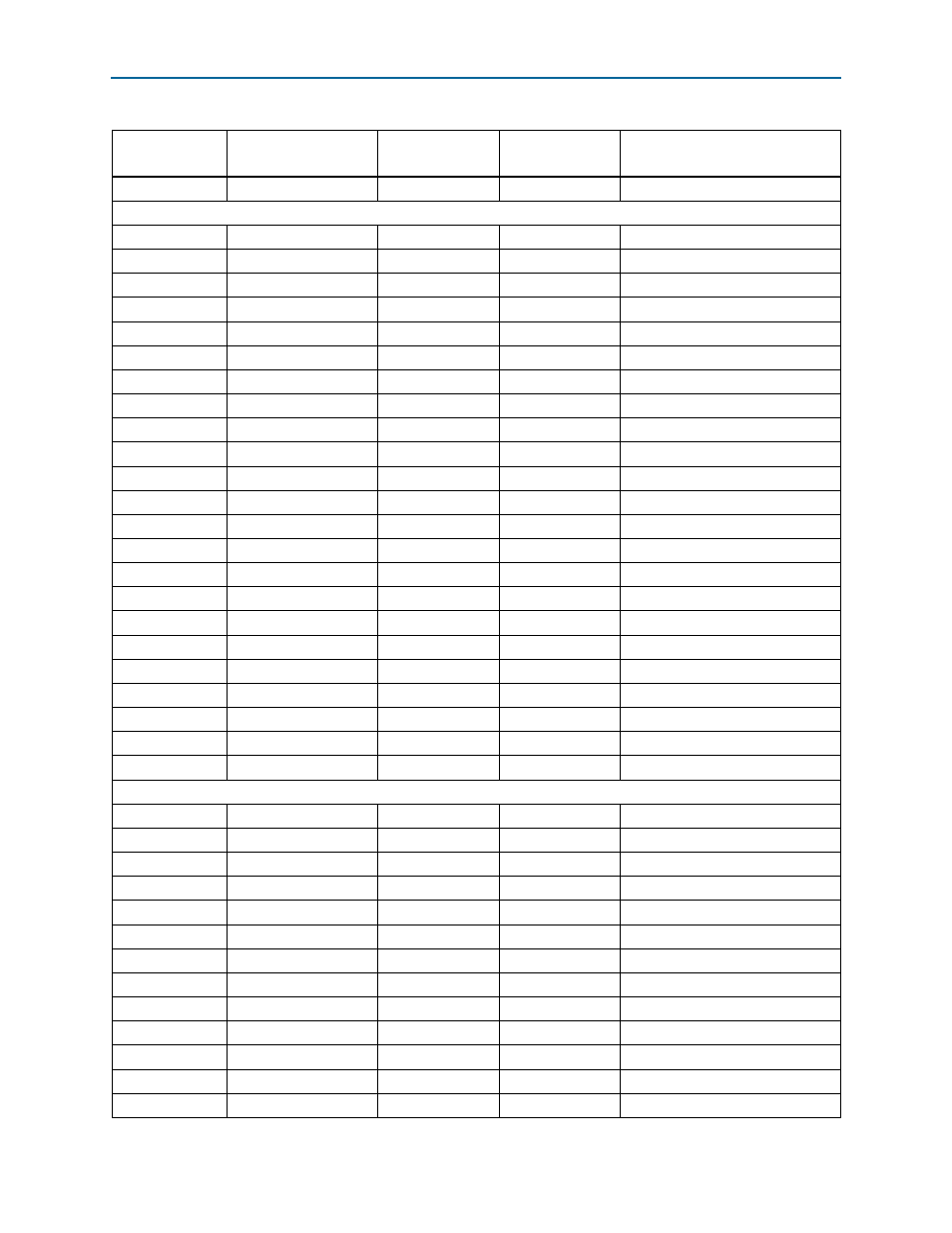
Table 2–31. DDR3A Devices Pin Assignments, Schematic Signal Names, and Functions (Part 4 of 5)
Board Reference
Schematic
Signal Name
Arria V GT FPGA
Pin Number
I/O Standard
Description