Memory, Ddr3, Ddr3a for fpga 1 – Altera Arria V GT FPGA Development Board User Manual
Page 64: Memory –54, Ddr3 –54, Ddr3a for fpga 1 –54
2–54
Chapter 2: Board Components
Memory
Arria V GT FPGA Development Board
December 2014
Altera Corporation
Reference Manual
Memory
This section describes the development board’s memory interface support and also
their signal names, types, and connectivity relative to the Arria V GT FPGA. The
development board has the following memory interfaces:
■
DDR3
■
QDRII+
■
Flash
f
For more information about the memory interfaces, refer to the following documents:
■
section in volume 4 of the External Memory Interface Handbook.
■
section in volume 6 of the
External Memory Interf
DDR3
DDR3A for FPGA 1
The development board supports a 16Mx72x8 bank DDR3 SDRAM interface on
FPGA 1 for very high-speed sequential memory access. The 72-bit data bus consists of
four x16 devices and one x8 device with a single address or command bus. This
interface connects to the vertical I/O banks on the top edge of the FPGA and utilizes
the memory soft controller.
This memory interface is designed to run at a target frequency of 667 MHz for a
maximum theoretical bandwidth of over 115.2 Gbps. The minimum frequency for this
device is 667 MHz. The target Micron device is rated at 800 MHz with a CAS latency
of 11.
16
SMA_B_10G_RX_P1
H39
LVDS or 2.5-V Transceiver channel
5
SMA_B_6G_RX_N0
AC2
LVDS or 2.5-V Transceiver channel
6
SMA_B_6G_RX_P0
AC1
LVDS or 2.5-V Transceiver channel
19
SMA_B_TX_L15_N
G36
LVDS or 2.5-V Transceiver channel
20
SMA_B_TX_L15_P
G37
LVDS or 2.5-V Transceiver channel
10
SMA_B_TX_R6_N
AB4
LVDS or 2.5-V Transceiver channel
14
SMA_B_TX_R6_P
AB3
LVDS or 2.5-V Transceiver channel
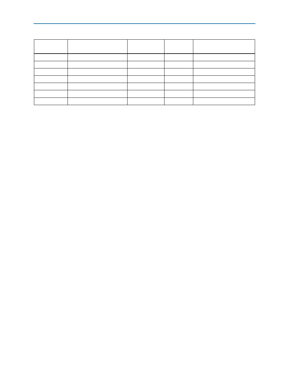
Table 2–30. Bull’s Eye Connector Pin Assignments, Schematic Signal Names, and Functions
Board
Reference (J16)
Schematic Signal Name
Arria V GT FPGA
Pin Number
I/O Standard
Description