Development board block diagram, Handling the board – Altera Cyclone V GT FPGA Development Board User Manual
Page 8

1–4
Chapter 1: Overview
Development Board Block Diagram
Cyclone V GT FPGA Development Board
September 2014
Altera Corporation
Reference Manual
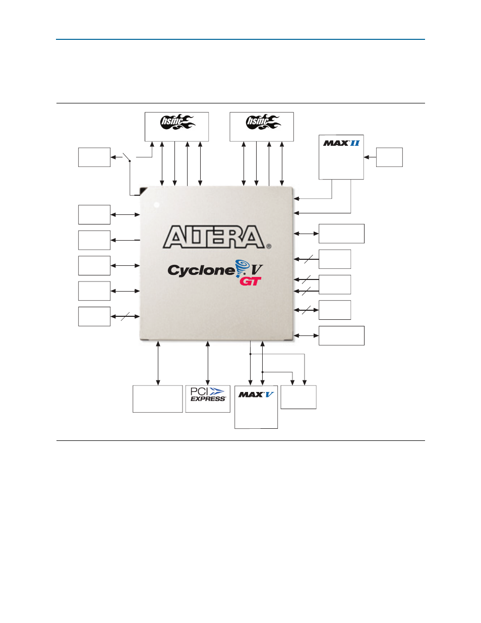
Development Board Block Diagram
shows a block diagram of the Cyclone V GT FPGA development board.
Handling the Board
When handling the board, it is important to observe the following static discharge
precaution:
c
Without proper anti-static handling, the board can be damaged. Therefore, use
anti-static handling precautions when touching the board.
Figure 1–1. Cyclone V GT FPGA Development Board Block Diagram
ASSP
CPLD
SMA
Clock Output
Gigabit
Ethernet PHY
LCD
DDR3
SMC x64
64
(Optional)
SMA Differential
Pair Clock Input
DDR3
HMC x40
Buttons
Switches
LED
Configuration
Interface EPCQ/CvP
8
4
40
8
On-Board
USB-Blaster II
and USB Interface
Mini-USB
Version 2.0
Tr
ansceiv
er x4
CLK
OUT
CLKIN
x32 DQ
Tr
ansceiv
er x3
CLK
OUT x3
CLKIN x3
x80
Port A LVDS
Port B x32 DQ/DQS
Transceiver x1
Resistor Stuffing
Option with HSMA
Populated by Default
JTAG Chain
x19 USB Interface
Oscillators
50 MHz, 125 MHz,
and Programmable
Tr
ansceiv
er x4
x4 Edge
ADDR
x16
1 Gbyte
Flash
5M2210ZF256C4N
SDI x1
TX/RX
)
5CGTFD9E5F35
