Fpga programming from flash memory, Fpga programming from flash memory –13 – Altera Cyclone V GT FPGA Development Board User Manual
Page 21
Chapter 2: Board Components
2–13
FPGA Configuration
September 2014
Altera Corporation
Cyclone V GT FPGA Development Board
Reference Manual
FPGA Programming from Flash Memory
Flash memory programming is possible through a variety of methods. The default
method is to use the factory design—Board Update Portal. This design is an
embedded web server, which serves the Board Update Portal web page. The web
page allows you to select new FPGA designs including hardware, software, or both in
an industry-standard S-Record File (.flash) and write the design to the user hardware
page (page 1) of the flash memory over the network.
The secondary method is to use the pre-built parallel flash loader (PFL) design
included in the development kit. The development board implements the Altera PFL
megafunction for flash memory programming. The PFL megafunction is a block of
logic that is programmed into an Altera programmable logic device (FPGA or CPLD).
The PFL functions as a utility for writing to a compatible flash memory device. This
pre-built design contains the PFL megafunction that allows you to write either page 0,
page 1, or other areas of flash memory over the USB interface using the Quartus II
software. This method is used to restore the development board to its factory default
settings.
Other methods to program the flash memory can be used as well, including the
Nios
®
II processor.
f
For more information on the Nios II processor, refe
of
the Altera website.
On either power-up or by pressing the program configuration push button,
PGM_CONFIG
(S5), the MAX V CPLD 5M2210 System Controller's PFL configures the
FPGA from the flash memory. The PFL megafunction reads 16-bit data from the flash
memory and converts it to fast passive parallel (FPP) format. This 8-bit data is then
written to the dedicated configuration pins in the FPGA during configuration.
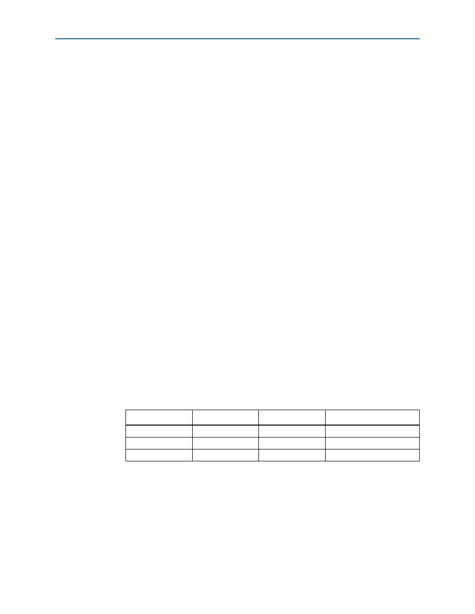
Pressing the PGM_CONFIG push button (S5) loads the FPGA with a design page based
on which PGM_LED[2:0] (D12, D13, D14) illuminates. You can select the design stored
in the flash by pressing the PGM_SEL push button (S6) to cycle through the LEDs as
defined in
.
lists the design that loads when you press the PGM_CONFIG push button.
Table 2–6. PGM_LED Settings
PGM_LED0 (D14)
PGM_LED1 (D13)
PGM_LED2 (D12)
Design
ON
OFF
OFF
Factory design
OFF
ON
OFF
User design 1
OFF
OFF
ON
User design 2
Note to
:
(1) ON indicates a setting of ’0’ while OFF indicates a setting of ’1’.