Off-board clock input/output, Off-board clock input/output –20 – Altera Cyclone V GT FPGA Development Board User Manual
Page 28
2–20
Chapter 2: Board Components
Clock Circuitry
Cyclone V GT FPGA Development Board
September 2014
Altera Corporation
Reference Manual
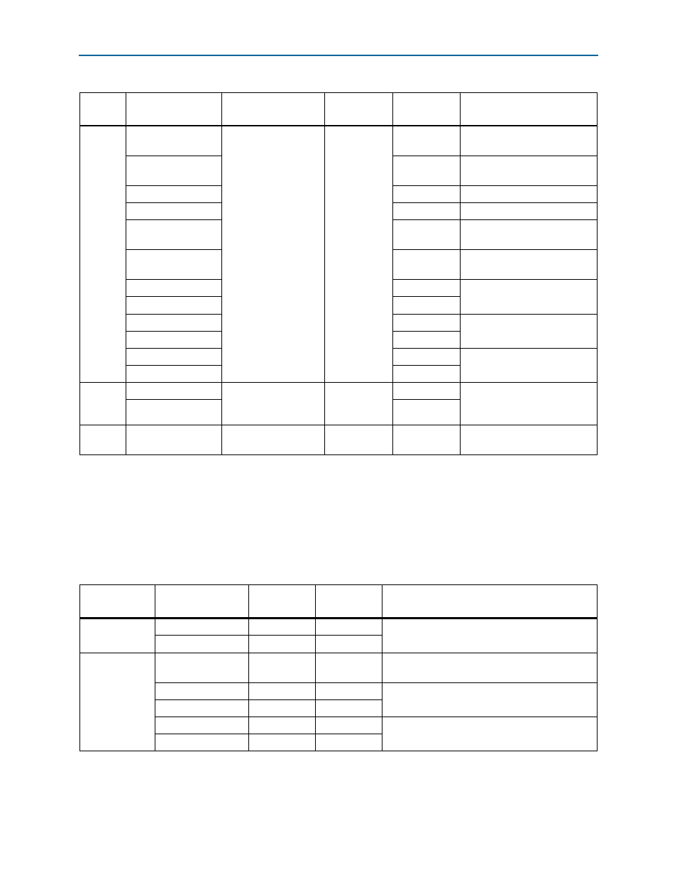
Off-Board Clock Input/Output
The development board has input and output clocks which can be driven onto the
board. The output clocks can be programmed to different levels and I/O standards
according to the FPGA device’s specification.
lists the clock inputs for the development board.
X4 to U3
CLKINTOP_P
100.000 MHz
(Programmable
between 10–810 MHz)
LVDS
(fanout
buffer)
H19
Top edge (CLK10p) for general
purpose logic
CLKINTOP_N
H18
Top edge (CLK10n) for general
purpose logic
CLKINBOT_P
AF18
Bottom edge (CLK2p)
CLKINBOT_N
AG18
Bottom edge (CLK2n)
CLKIN_R_P
W26
Right edge (CLK7p) for general
purpose logic
CLKIN_R_N
W27
Right edge (CLK7n) for general
purpose logic
REFCLK_QL1_P
AA11
Transceiver bank QL0 for PCI
Express edge connector
REFCLK_QL1_N
AB10
REFCLK_QL3_P
R11
Transceiver bank QL3 for
HSMC port B transceivers
REFCLK_QL3_N
P10
SMA_CLKOUT_P
—
Oscilloscope trigger output
SMA_CLKOUT_N
—
X3
REFCLK_QL2_P
148.500 MHz
(Programmable
between 10–810 MHz)
LVDS
U11
SDI video or HSMC port A
transceivers
REFCLK_QL2_N
T10
X1
ENET_XTAL_25MHZ
25.000 MHz
2.5-V CMOS
—
Reference clock for the
Ethernet PHY
Table 2–11. On-Board Oscillators (Part 2 of 2)
Source
Schematic Signal
Name
Frequency
I/O Standard
Cyclone V GT
Pin Number
Application
Table 2–12. Off-Board Clock Inputs (Part 1 of 2)
Source
Schematic Signal
Name
I/O Standard
Cyclone V GT
Pin Number
Description
SMA
CLKIN_SMA_P
LVPECL
—
Input to LVDS fan-out buffer (drives two reference
clocks and three GPLL inputs)
CLKIN_SMA_N
LVPECL
—
Samtec HSMC
HSMA_CLK_IN0
2.5-V
G11
Single-ended input from the installed HSMC cable
or board.
HSMA_CLK_IN_P1
LVDS/2.5-V
G18
LVDS input from the installed HSMC cable or
board. Can also support 2x LVTTL inputs.
HSMA_CLK_IN_N1
LVDS/LVTTL
F18
HSMA_CLK_IN_P2
LVDS/LVTTL
H17
LVDS input from the installed HSMC cable or
board. Can also support 2x LVTTL inputs.
HSMA_CLK_IN_N2
LVDS/LVTTL
H16