Ddr3b, Ddr3b –42 – Altera Cyclone V GT FPGA Development Board User Manual
Page 50
2–42
Chapter 2: Board Components
Memory
Cyclone V GT FPGA Development Board
September 2014
Altera Corporation
Reference Manual
DDR3B
The DDR3B SDRAM comprises of four ×16 devices with a single address and
command bus. This interface connects to the horizontal I/O banks on the right edge
of the FPGA and utilizes the soft memory controller.
This memory interface runs at a target frequency of 300 MHz for a maximum
theoretical bandwidth of over 38.40 Gbps.
lists the DDR3B pin assignments, signal names, and functions. The signal
names and types are relative to the Cyclone V GT in terms of I/O setting and
direction.
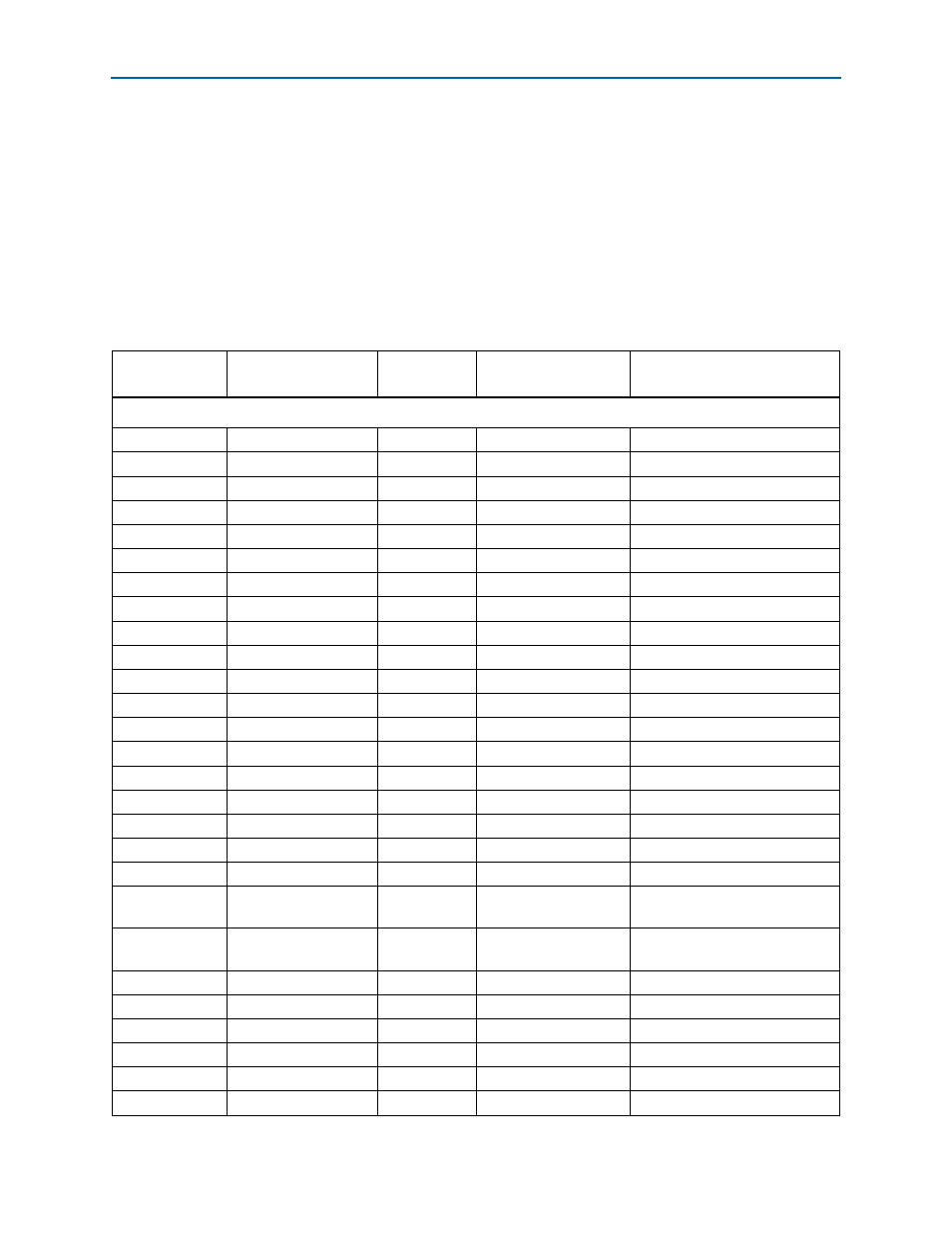
Table 2–29. DDR3B Device Pin Assignments, Schematic Signal Names, and Functions (Part 1 of 6)
Board Reference
Schematic
Signal Name
Cyclone V GT
Pin Number
I/O Standard
Description
DDR3 x16 (U30)
N3
DDR3B_A0
H29
1.5-V SSTL Class I
Address bus
P7
DDR3B_A1
K28
1.5-V SSTL Class I
Address bus
P3
DDR3B_A2
K34
1.5-V SSTL Class I
Address bus
N2
DDR3B_A3
L32
1.5-V SSTL Class I
Address bus
P8
DDR3B_A4
R32
1.5-V SSTL Class I
Address bus
P2
DDR3B_A5
R33
1.5-V SSTL Class I
Address bus
R8
DDR3B_A6
N32
1.5-V SSTL Class I
Address bus
R2
DDR3B_A7
G33
1.5-V SSTL Class I
Address bus
T8
DDR3B_A8
AE34
1.5-V SSTL Class I
Address bus
R3
DDR3B_A9
L27
1.5-V SSTL Class I
Address bus
L7
DDR3B_A10
V33
1.5-V SSTL Class I
Address bus
R7
DDR3B_A11
U33
1.5-V SSTL Class I
Address bus
N7
DDR3B_A12
T31
1.5-V SSTL Class I
Address bus
T3
DDR3B_A13
T30
1.5-V SSTL Class I
Address bus
M2
DDR3B_BA0
J31
1.5-V SSTL Class I
Bank address bus
N8
DDR3B_BA1
N29
1.5-V SSTL Class I
Bank address bus
M3
DDR3B_BA2
P27
1.5-V SSTL Class I
Bank address bus
K3
DDR3B_CASN
N27
1.5-V SSTL Class I
Row address select
K9
DDR3B_CKE
AF32
1.5-V SSTL Class I
Column address select
J7
DDR3B_CLK_P
R30
Differential 1.5-V SSTL
Class I
Differential output clock
K7
DDR3B_CLK_N
R29
Differential 1.5-V SSTL
Class I
Differential output clock
L2
DDR3B_CSN
V27
1.5-V SSTL Class I
Chip select
E7
DDR3B_DM0
AE30
1.5-V SSTL Class I
Write mask byte lane
D3
DDR3B_DM1
AE32
1.5-V SSTL Class I
Write mask byte lane
E3
DDR3B_DQ0
AF31
1.5-V SSTL Class I
Data bus byte lane 0
F7
DDR3B_DQ1
AD30
1.5-V SSTL Class I
Data bus byte lane 0
F2
DDR3B_DQ2
AJ32
1.5-V SSTL Class I
Data bus byte lane 0