Altera Cyclone V GT FPGA Development Board User Manual
Page 11
Chapter 2: Board Components
2–3
Board Overview
September 2014
Altera Corporation
Cyclone V GT FPGA Development Board
Reference Manual
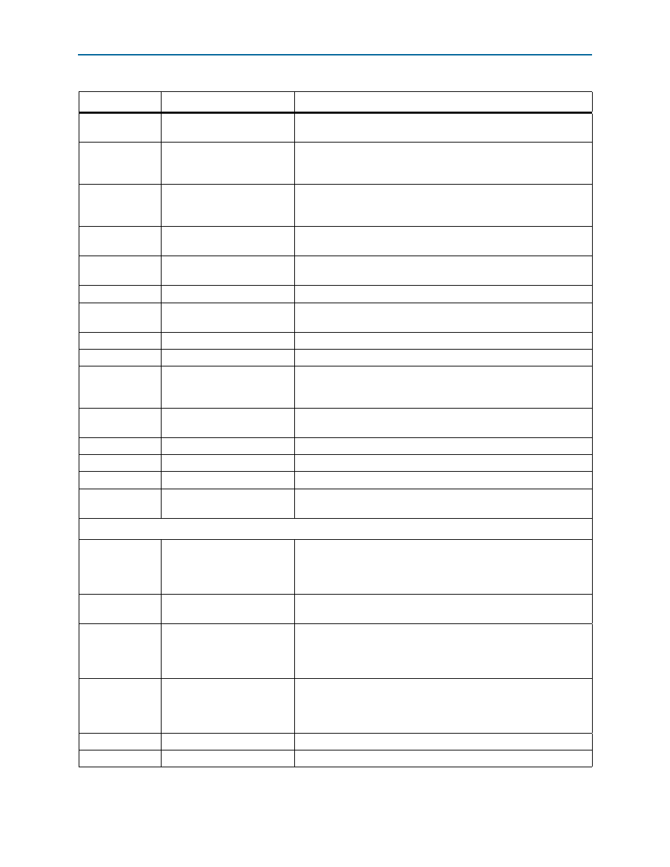
J5
Mini USB type-AB connector
USB interface for FPGA programming and debugging through the
embedded USB-Blaster II JTAG via a mini-USB type-B cable.
SW4
Board settings DIP switch
Controls the MAX V CPLD 5M2210 System Controller functions such
as clock enable, SMA clock input control, and which image to load
from flash memory at power-up.
SW5
FPGA configuration mode DIP
Switch
Controls the supported FPGA configuration mode by altering the MSEL
input pins. This switch can also control the fan speed by forcing it to
run at full speed, over-riding the fan control block in the MAX V CPLD.
S6
Program select push button
Toggles the program select LEDs, which selects the program image
that loads from flash memory to the FPGA.
S5
Program configuration push
button
Load image from flash memory to the FGPA based on the settings of
the program select LEDs.
D7
Configuration done LED
Illuminates when the FPGA is configured.
D6
Load LED
Illuminates when the MAX V CPLD 5M2210 System Controller is
actively configuring the FPGA.
D5
Error LED
Illuminates when the FPGA configuration from flash memory fails.
D21
Power LED
Illuminates when 5.0-V power is present.
D12, D13, D14
Program select LEDs
Illuminates to show the LED sequence that determines which flash
memory image loads to the FPGA when you press the program select
push button. Refer to
for the LED settings.
D22, D23, D24,
D25, D26
Ethernet LEDs
Illuminates to show the connection speed as well as transmit or
receive activity.
D32
SDI LEDs
Illuminates to show the transmit or receive activity.
D3, D4, D19, D20
HSMC port LEDs
You can configure these LEDs to indicate transmit or receive activity.
D1, D2
HSMC port present LED
Illuminates when a daughtercard is plugged into the HSMC port.
D34, D35, D44,
D45
PCI Express link LEDs
You can configure these LEDs to indicate the PCI Express link width
(x1, x4) and Gen1 link.
Clock Circuitry
X6
50-MHz oscillator
50.000-MHz crystal oscillator for general purpose logic. This oscillator
is the input source to a clock buffer with two outputs. One output clock
goes to the FPGA and one goes to the MAX V CPLD 5M2210 System
Controller.
X2
100-MHz oscillator
100.000-MHz crystal oscillator for the MAX V CPLD 5M2210 System
Controller.
X3
148.500-MHz oscillator
148.500-MHz voltage controlled oscillator for the serial digital
interface (SDI) video. This oscillator is programmable to any frequency
between 20–810 MHz using the clock control GUI running on the
MAX V CPLD 5M2210 System Controller.
X4
100-MHz oscillator
Programmable oscillator (10–810 MHz) with a default frequency of
100.000 MHz. This clock is the clock input source to a 6-output clock
buffer (U3). The buffer can select between this clock source or a pair of
SMA connectors as the input clock source.
X5
125-MHz oscillator
125.000-MHz voltage controlled oscillator for the FPGA.
J11, J12
SDI transceiver connectors
Drives serial data input/output to or from the SDI video port.
Table 2–1. Board Components (Part 2 of 4)
Board Reference
Type
Description