Fpga configuration, Fpga programming over embedded usb-blaster, Fpga configuration –11 – Altera Cyclone V GT FPGA Development Board User Manual
Page 19: Fpga programming over embedded usb-blaster –11
Chapter 2: Board Components
2–11
FPGA Configuration
September 2014
Altera Corporation
Cyclone V GT FPGA Development Board
Reference Manual
FPGA Configuration
The Cyclone V GT development board supports the following three configuration
methods:
■
Embedded USB-Blaster II is the default method for configuring the FPGA using
the Quartus II Programmer in JTAG mode with the supplied USB cable.
■
Flash memory download for configuring the FPGA using stored images from the
flash memory on either power-up or pressing the program configuration
push button (S6).
■
External USB-Blaster for configuring the FPGA using an external USB-Blaster that
connects to the JTAG chain header (J13).
FPGA Programming over Embedded USB-Blaster
This configuration method implements a type-B mini USB connector (J5), a USB 2.0
PHY device (U4), and an Altera MAX II CPLD EPM570GT100C3N (U49) to allow
FPGA configuration using a USB cable. This USB cable connects directly between the
USB connector on the board and a USB port of a PC running the Quartus II software.
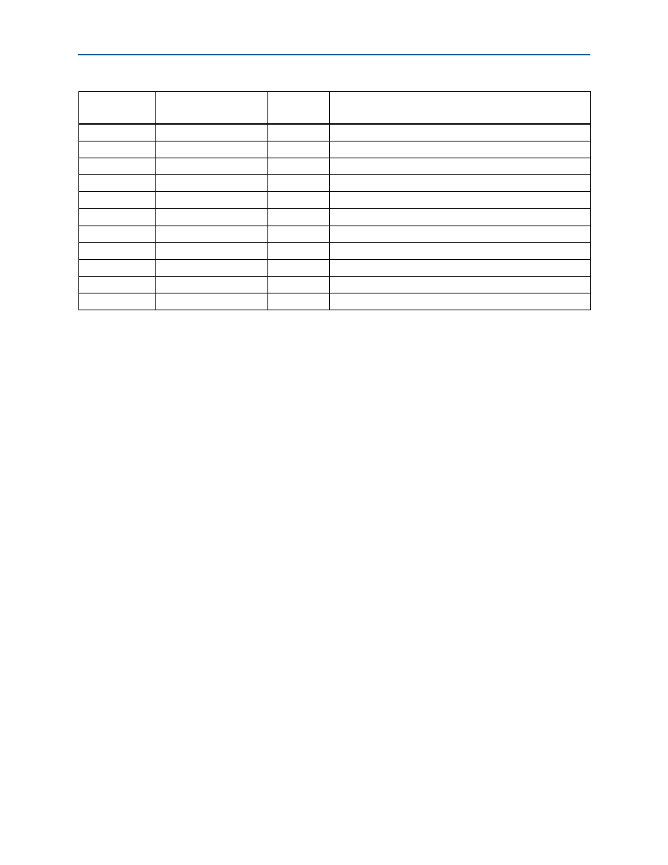
P8
USB_CFG2
1.8-V
Embedded USB-Blaster II interface. Reserved for future use
T7
USB_CFG3
1.8-V
Embedded USB-Blaster II interface. Reserved for future use
N8
USB_CFG4
1.8-V
Embedded USB-Blaster II interface. Reserved for future use
R8
USB_CFG5
1.8-V
Embedded USB-Blaster II interface. Reserved for future use
T8
USB_CFG6
1.8-V
Embedded USB-Blaster II interface. Reserved for future use
T9
USB_CFG7
1.8-V
Embedded USB-Blaster II interface. Reserved for future use
R9
USB_CFG8
1.8-V
Embedded USB-Blaster II interface. Reserved for future use
P9
USB_CFG9
1.8-V
Embedded USB-Blaster II interface. Reserved for future use
M8
USB_CFG10
1.8-V
Embedded USB-Blaster II interface. Reserved for future use
T10
USB_CFG11
1.8-V
Embedded USB-Blaster II interface. Reserved for future use
H5
USB_CLK
2.5-V
Embedded USB-Blaster II interface clock
Table 2–5. MAX V CPLD 5M2210 System Controller Device Pin-Out (Part 5 of 5)
Board
Reference (U32)
Schematic Signal Name
I/O Standard
Description