Sdi channel (optional), Sdi channel (optional) –34 – Altera Cyclone V GT FPGA Development Board User Manual
Page 42
2–34
Chapter 2: Board Components
Components and Interfaces
Cyclone V GT FPGA Development Board
September 2014
Altera Corporation
Reference Manual
SDI Channel (Optional)
The development board is fully populated with the serial digital interface (SDI)
channel. However, this interface shares a transceiver channel with the HSMC port A
(transceiver channel 3) through a resistor-stuffing option. By default, the resistors are
populated such that the HSMC port A transceiver is enabled.
1
If you enable the SDI interface, the HSMC port A transceiver channel 3 will be
disabled.
80
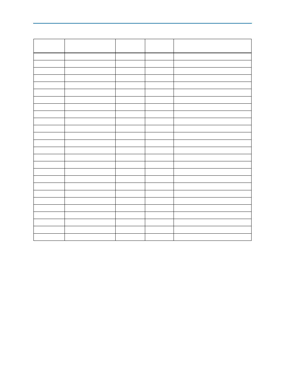
HSMB_A7
D22
2.5-V CMOS
Memory address bus
84
HSMB_A8
D19
2.5-V CMOS
Memory address bus
86
HSMB_A9
B21
2.5-V CMOS
Memory address bus
102
HSMB_DM2
C31
2.5-V CMOS
Data mask
104
HSMB_A10
E20
2.5-V CMOS
Memory address bus
108
HSMB_A11
B23
2.5-V CMOS
Memory address bus
110
HSMB_A12
L25
2.5-V CMOS
Memory address bus
114
HSMB_A13
B19
2.5-V CMOS
Memory address bus
116
HSMB_A14
B20
2.5-V CMOS
Memory address bus
126
HSMB_DM3
H27
2.5-V CMOS
Data mask
128
HSMB_A15
A21
2.5-V CMOS
Memory address bus
132
HSMB_BA0
B26
2.5-V CMOS
Memory bank address bus
134
HSMB_BA1
A27
2.5-V CMOS
Memory bank address bus
138
HSMB_BA2
D20
2.5-V CMOS
Memory bank address bus
140
HSMB_BA3
M19
2.5-V CMOS
Memory bank address bus
68
HSMB_DQS_N0
M21
2.5-V CMOS
Memory data strobe
92
HSMB_DQS_N1
N23
2.5-V CMOS
Memory data strobe
122
HSMB_DQS_N2
K23
2.5-V CMOS
Memory data strobe
146
HSMB_DQS_N3
N24
2.5-V CMOS
Memory data strobe
66
HSMB_DQS_P0
N22
2.5-V CMOS
Memory data strobe
90
HSMB_DQS_P1
M23
2.5-V CMOS
Memory data strobe
120
HSMB_DQS_P2
L23
2.5-V CMOS
Memory data strobe
144
HSMB_DQS_P3
M24
2.5-V CMOS
Memory data strobe
150
HSMB_CKE
C22
2.5-V CMOS
Memory clock enable
152
HSMB_CSN
M25
2.5-V CMOS
Chip select
160
HSMB_PRSNTN
M20
2.5-V CMOS
HSMC port B presence detect
Table 2–22. HSMC Interface Pin Assignments, Schematic Signal Names, and Functions (Part 6 of 6)
Board
Reference
Schematic Signal Name
Cyclone V GT
Pin Number
I/O Standard
Description