User-defined dip switch, User-defined leds, General leds – Altera Cyclone V GT FPGA Development Board User Manual
Page 30: User-defined dip switch –22 user-defined leds –22, General leds –22
2–22
Chapter 2: Board Components
General User Input/Output
Cyclone V GT FPGA Development Board
September 2014
Altera Corporation
Reference Manual
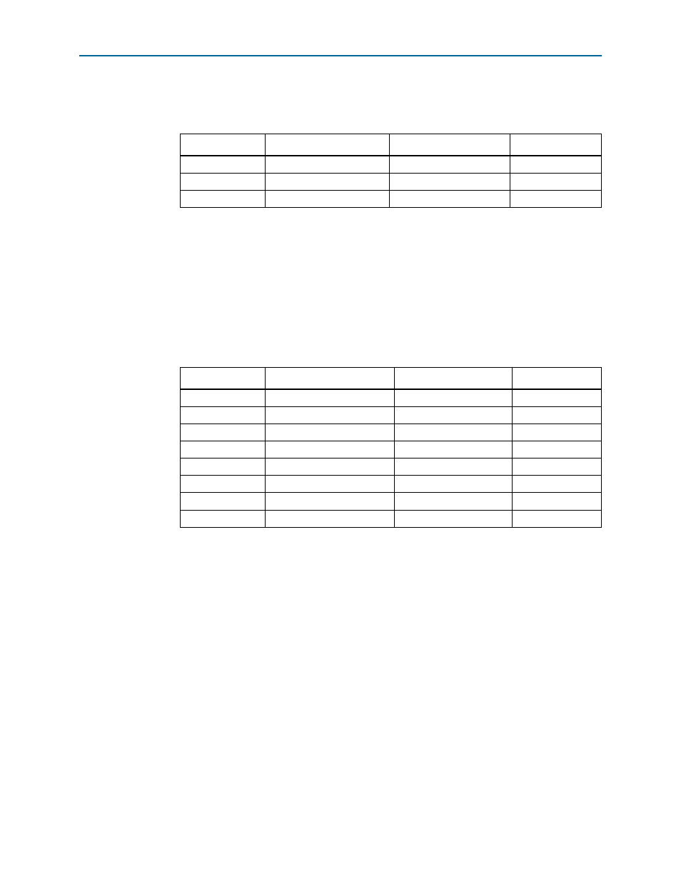
lists the user-defined push button schematic signal names and their
corresponding Cyclone V GT device pin numbers.
User-Defined DIP Switch
Board reference SW1 is a eight-pin DIP switch. This switch is user-defined and
provides additional FPGA input control. When the switch is in the OFF position, a
logic 1 is selected. When the switch is in the ON position, a logic 0 is selected. There
are no board-specific functions for this switch.
lists the user-defined DIP switch schematic signal names and their
corresponding Cyclone V GT device pin numbers.
User-Defined LEDs
The development board includes general and HSMC user-defined LEDs. This section
describes all user-defined LEDs. For information on board specific or status LEDs,
refer to
“Status Elements” on page 2–15
General LEDs
Board references D8–D11 and D15–D18 are eight user-defined LEDs. The status and
debugging signals are driven to the LEDs from the designs loaded into the
Cyclone V GT device. Driving a logic 0 on the I/O port turns the LED on while
driving a logic 1 turns the LED off. There are no board-specific functions for these
LEDs.
Table 2–14. User-Defined Push Button Schematic Signal Names and Functions
Board Reference
Schematic Signal Name
Cyclone V GT Pin Number
I/O Standard
S3
USER_PB0
AK13
2.5-V
S2
USER_PB1
AA15
2.5-V
S1
USER_PB2
AN8
2.5-V
Table 2–15. User-Defined DIP Switch Schematic Signal Names and Functions
Board Reference
Schematic Signal Name
Cyclone V GT Pin Number
I/O Standard
1
USER_DIPSW0
H12
2.5-V
2
USER_DIPSW1
A2
2.5-V
3
USER_DIPSW2
E10
2.5-V
4
USER_DIPSW3
D9
2.5-V
5
USER_DIPSW4
E9
2.5-V
6
USER_DIPSW5
D7
2.5-V
7
USER_DIPSW6
E8
2.5-V
8
USER_DIPSW7
E7
2.5-V