Altera Cyclone V GT FPGA Development Board User Manual
Page 33
Chapter 2: Board Components
2–25
Components and Interfaces
September 2014
Altera Corporation
Cyclone V GT FPGA Development Board
Reference Manual
The power for the board can be sourced entirely from the PCI Express edge connector
when installed into a PC motherboard. Although the board can also be powered by a
laptop power supply for use on a lab bench, Altera recommends that you do not
power up from both supplies at the same time. Ideal diode power sharing devices
have been designed into this board to prevent damages or back-current from one
supply to the other.
The PCIE_REFCLK_P/N signal is a 100 MHz differential input that is driven from the PC
motherboard on to this board through the edge connector. This signal connects
directly to a Cyclone V GT REFCLK input pin pair using DC coupling. This clock is
terminated on the motherboard and therefore, no on-board termination is required.
This clock can have spread-spectrum properties that change its period between
9.847 ps to 10.203 ps. The I/O standard is High-Speed Current Steering Logic (HCSL).
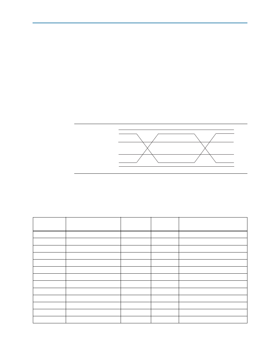
shows the PCI Express reference clock levels.
The SMB connections are optional signals in the PCI Express specification. The signals
are wired to the Cyclone V GT device but are not required for normal operation.
summarizes the PCI Express pin assignments. The signal names and
directions are relative to the Cyclone V GT device.
Figure 2–6. PCI Express Reference Clock Levels
V
MAX
= 1.15 V
V
CROSS MAX
= 550 mV
V
CROSS MIN
= 250 mV
V
MIN
= –0.30 V
REFCLK –
REFCLK +
Table 2–20. PCI Express Pin Assignments, Schematic Signal Names, and Functions (Part 1 of 2)
Board
Reference (J16)
Schematic Signal Name
Cyclone V GT
Pin Number
I/O Standard
Description
A11
PCIE_PERSTN
AA22
LVTTL
Reset
A1
PCIE_PRSNT1N
—
LVTTL
Link width DIP switch
B17
PCIE_PRSNT2N_X1
—
LVTTL
Hot plug present detect
B31
PCIE_PRSNT2N_X4
—
LVTTL
Hot plug present detect
A13
PCIE_REFCLK_P
W11
HCSL
Reference clock input
A14
PCIE_REFCLK_N
V10
HCSL
Reference clock input
B14
PCIE_RX_P0
AJ2
1.5-V PCML
Receive bus
B15
PCIE_RX_N0
AJ1
1.5-V PCML
Receive bus
B19
PCIE_RX_P1
AG2
1.5-V PCML
Receive bus
B20
PCIE_RX_N1
AG1
1.5-V PCML
Receive bus
B23
PCIE_RX_P2
AE2
1.5-V PCML
Receive bus
B24
PCIE_RX_N2
AE1
1.5-V PCML
Receive bus
B27
PCIE_RX_P3
AC2
1.5-V PCML
Receive bus