Memory, Ddr3 sdram, Ddr3a – Altera Cyclone V GT FPGA Development Board User Manual
Page 45: Memory –37, Ddr3 sdram –37, Ddr3a –37
Chapter 2: Board Components
2–37
Memory
September 2014
Altera Corporation
Cyclone V GT FPGA Development Board
Reference Manual
Memory
This section describes the development board’s memory interface support and also
their signal names, types, and connectivity relative to the Cyclone V GT. The
development board has the following memory interfaces:
■
DDR3 SDRAM
■
Synchronous flash
f
For more information about the memory interfaces, refer to the following documents:
■
section in the External Memory Interface Handbook.
■
section in the External Memory
Interface Handbook.
DDR3 SDRAM
The development board supports seven 16Mx16x8 DDR3 SDRAM interfaces for very
high-speed sequential memory access. The DDR3 SDRAM has two independent
interfaces:
■
DDR3A—40-bit data interface using a hard memory controller. This data bus
consists of three ×16 devices and one of which only uses the first 8-bits of the ×8
device for ECC support.
■
DDR3B—64-bit interface using a soft memory controller. This data bus consists of
four ×16 devices.
DDR3A
The DDR3A SDRAM comprises of three ×16 devices with a single address and
command bus. This interface connects to the vertical I/O banks on the bottom edge of
the FPGA and utilizes the hard memory controller.
This memory interface runs at a target frequency of 400 MHz for a maximum
theoretical bandwidth of over 32 Gbps.
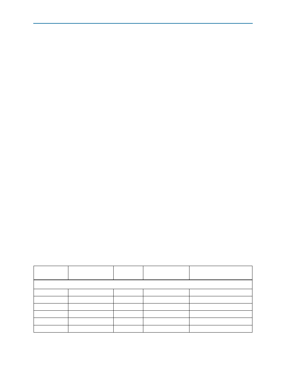
lists the DDR3A pin assignments, signal names, and functions. The signal
names and types are relative to the Cyclone V GT in terms of I/O setting and
direction.
Table 2–28. DDR3A Device Pin Assignments, Schematic Signal Names, and Functions (Part 1 of 5)
Board Reference
Schematic
Signal Name
Cyclone V GT
Pin Number
I/O Standard
Description
DDR3 x16 (U26)
N3
DDR3A_A0
AK18
1.5-V SSTL Class I
Address bus
P7
DDR3A_A1
AL18
1.5-V SSTL Class I
Address bus
P3
DDR3A_A2
AM18
1.5-V SSTL Class I
Address bus
N2
DDR3A_A3
AN18
1.5-V SSTL Class I
Address bus
P8
DDR3A_A4
AH17
1.5-V SSTL Class I
Address bus
P2
DDR3A_A5
AJ17
1.5-V SSTL Class I
Address bus