Featured device: cyclone v gt fpga, I/o resources, Featured device: cyclone v gt fpga –5 – Altera Cyclone V GT FPGA Development Board User Manual
Page 13: I/o resources –5
Chapter 2: Board Components
2–5
Featured Device: Cyclone V GT FPGA
September 2014
Altera Corporation
Cyclone V GT FPGA Development Board
Reference Manual
Featured Device: Cyclone V GT FPGA
The Cyclone V GT FPGA development board features a Cyclone V GT
5CGTFD9E5F35C7N device in a 1152-pin FBGA package.
f
For more information about Cyclone V device family, refe
describes the features of the Cyclone V GT 5CGTFD9E5F35C7N device.
I/O Resources
The Cyclone V GT 5CGTFD9E5F35C7N device has total of 560 user I/Os and 12
transceiver channels.
lists the Cyclone V GT device I/O pin count and usage
by function on the board.
SW2
Power switch
Switch to power on or off the board when power is supplied from the
DC input jack.
J15
Fan power
Fan power header.
Table 2–1. Board Components (Part 4 of 4)
Board Reference
Type
Description
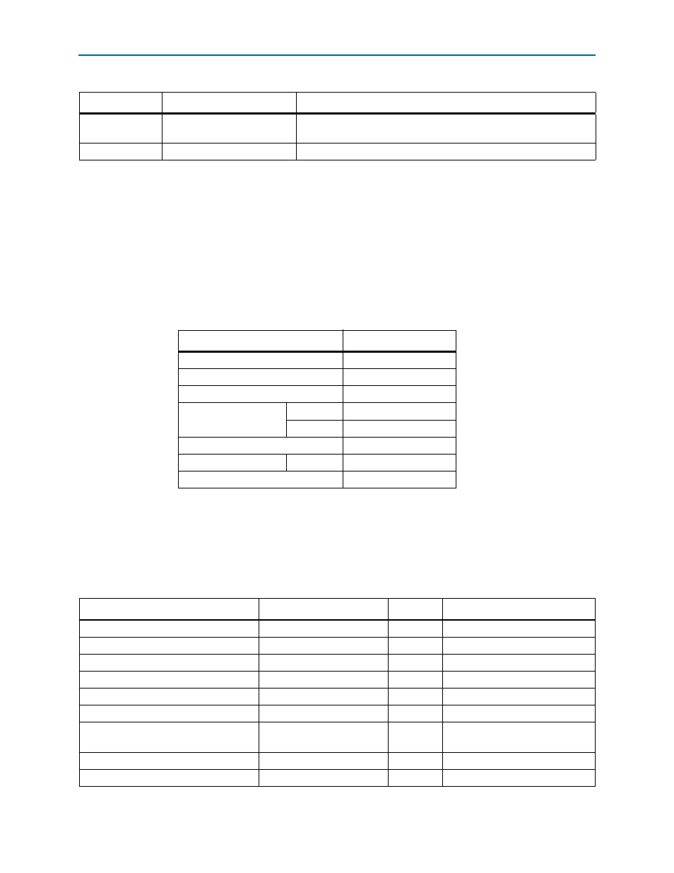
Table 2–2. Cyclone V GT Features
Resource
5CGTFD9E5F35C7N
LEs (K)
301
ALMs
113,560
Register
454,240
Memory (Kb)
M10K
12,200
MLAB
1,717
18-bit × 18-bit Multiplier
684
PLLs
8
Transceivers (6 Gbps)
12
Table 2–3. Cyclone V GT Device I/O Pin Count
Function
I/O Standard
I/O Count
Special Clock Pins
DDR3A
1.5-V SSTL
81
—
DDR3B
1.5-V SSTL
114
—
MAX V System Controller
1.8-V CMOS
4
—
Flash
1.8-V CMOS
49
—
PCI Express x4 port
2.5-V CMOS
8
One reference clock
HSMA port
2.5-V CMOS + LVDS
87
—
HSMB port
1.2-V–2.5-V CMOS DQ/DQS
(Default: 2.5-V)
88
—
Gigabit Ethernet port
2.5-V CMOS + LVDS
16
—
On-Board USB-Blaster II
1.5-V or 2.5-V CMOS
19
—