Sdi video input, Sdi video input –36 – Altera Cyclone V GT FPGA Development Board User Manual
Page 44
2–36
Chapter 2: Board Components
Components and Interfaces
Cyclone V GT FPGA Development Board
September 2014
Altera Corporation
Reference Manual
SDI Video Input
The cable equalizer supports operation at 270 Mb SD, 1.5 Gb HD, and 2.97 Gb dual-
link HD modes. Control signals are allowed for bypassing or disabling the device, as
well as a carrier detect or auto-mute signal interface.
lists the cable equalizer lengths.
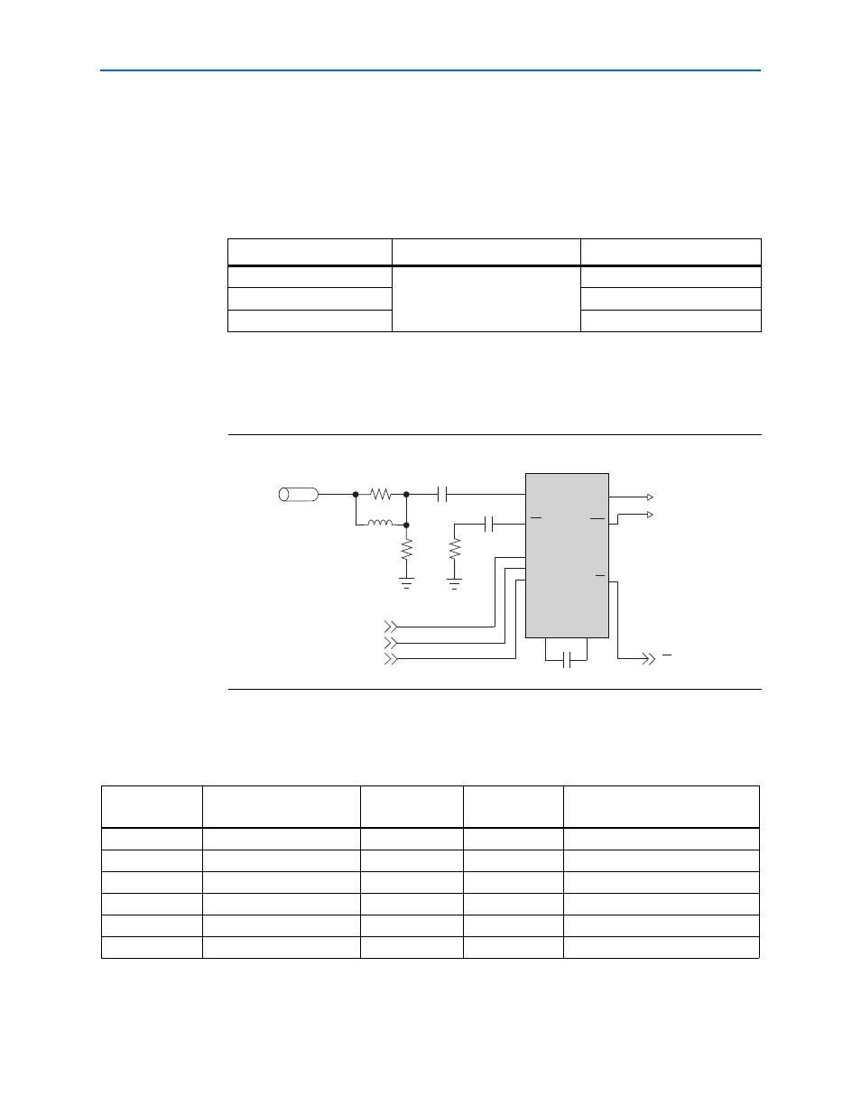
shows the SDI cable equalizer, which is an excerpt from the LMH0384
cable equalizer data sheet. On this development board, the output is a single-ended
output, with the negative channel driving a load local to the board.
summarizes the SDI video input interface pin assignments, signal names,
and functions.
Table 2–26. SDI Cable Equalizer Lengths
Data Rate (Mbps)
Cable Type
Maximum Cable Length (m)
270
Belden 1694A
400
1485
140
2970
120
Figure 2–9. SDI Cable Equalizer
BYPASS
MUTE
REF
1.0
μF
75
Ω
37.4
Ω
1.0
μF
1.0
μF
CD
SDI
SDI
SDO
SDO
CD
MUTE
MUTE
REF
BYPASS
AEC+
AEC–
75
Ω
MUTE
Coaxial Cable
SDI Adaptive
Cable Equalizer
To FPGA
5.6 nH
Table 2–27. SDI Video Input Interface Pin Assignments, Schematic Signal Names, and Functions
Board
Reference (U47)
Schematic Signal Name
Cyclone V GT
Pin Number
I/O Standard
Description
2
SDI_A_IN_P1
—
2.5-V
Serial data
3
SDI_A_EQIN_N1
—
2.5-V
Serial data
7
SDI_A_RX_BYPASS
AM9
2.5-V
Equalizer bypass enable
10
SDI_A_RX_N
R1
1.5-V PCML
Serial data input N
11
SDI_A_RX_P
R2
1.5-V PCML
Serial data input P
14
SDI_A_RX_EN
AN4
2.5-V
Device enable