Hsmc, Hsmc –28 – Altera Cyclone V GT FPGA Development Board User Manual
Page 36
2–28
Chapter 2: Board Components
Components and Interfaces
Cyclone V GT FPGA Development Board
September 2014
Altera Corporation
Reference Manual
HSMC
The development board supports two HSMC interfaces. Each physical interface
provides four channels of 5.0 Gbps-capable transceivers. The HSMC port A interface
supports both single-ended and differential signaling. The HSMC port B is a new
DQS standard to support both single-ended signaling and external memory
interfaces.
The HSMC port A interface supports a full SPI4.2 interface (17 LVDS channels), three
input and output clocks, as well as JTAG and SMB signals. The LVDS channels can be
used for CMOS signaling or LVDS.
The HSMC port B interface, other than supporting three input and output clocks as
well as SMBus and JTAG signals, it also covers the new DQS standard to support
daughtercards with external memory devices. For memory support, the VCCIO banks
for the HSMC port B is adjustable between 1.2 V, 1.5 V, 1.8 V, and 2.5 V. When the DQS
features are not used, these channels can be used for CMOS signaling.
1
The HSMC is an Altera-developed open specification, which allows you to expand
the functionality of the development board through the addition of daughtercards
(HSMCs).
f
For more information about the HSMC specification such as signaling standards,
signal integrity, compatible connectors, and mechanical information, refer to the
manual.
The HSMC connector has a total of 172 pins, including 120 signal pins, 39 power pins,
and 13 ground pins. The ground pins are located between the two rows of signal and
power pins, acting both as a shield and a reference. The HSMC host connector is
based on the 0.5 mm-pitch QSH/QTH family of high-speed, board-to-board
connectors from Samtec. There are three banks in this connector. Bank 1 has every
third pin removed as done in the QSH-DP/QTH-DP series. Bank 2 and bank 3 have
all the pins populated as done in the QSH/QTH series.
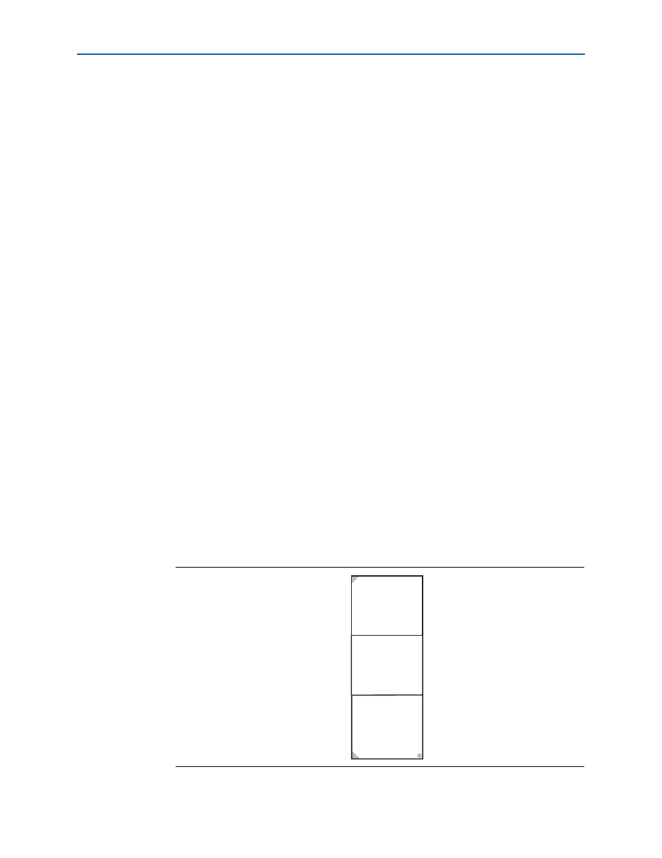
shows the bank arrangement of signals with respect to the Samtec
connector's three banks.
Figure 2–8. HSMC Signal and Bank Diagram
Bank 3
Power
D(79.40)
-or-
LVDS
CLKIN2, CLKOUT2
Bank 2
Power
D(39:0)
-or-
D[3:0] + LVDS
CLKIN1, CLKOUT1
Bank 1
8 TX Channels CDR
8 RX Channels CDR
JTAG
SMB
CLKIN0, CLKOUT0