Power measurement, Power measurement –51 – Altera Cyclone V GT FPGA Development Board User Manual
Page 59
Chapter 2: Board Components
2–51
Power Supply
September 2014
Altera Corporation
Cyclone V GT FPGA Development Board
Reference Manual
Power Measurement
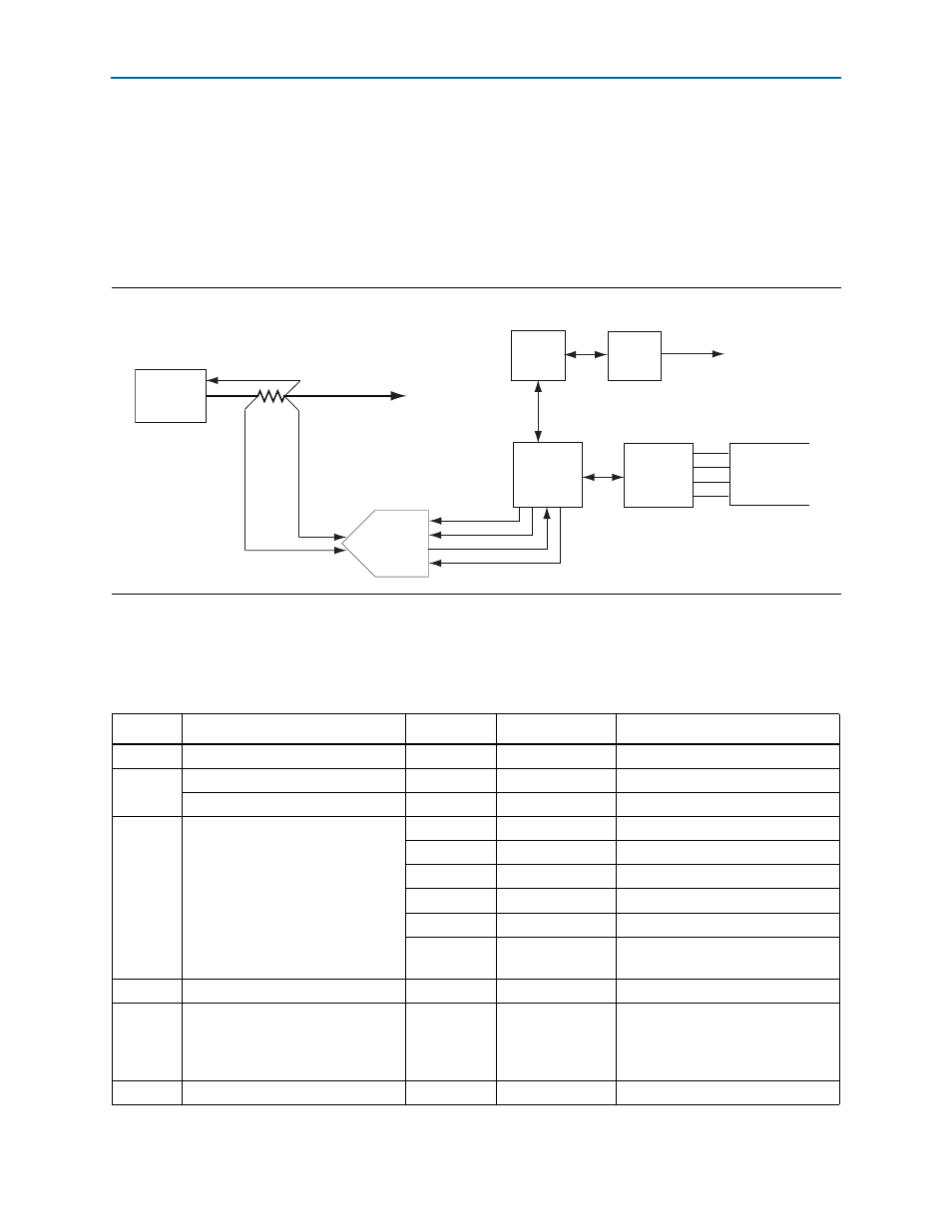
There are six power supply rails that have on-board current sense capabilities using
24-bit differential ADC devices. Precision sense resistors split the ADC devices and
rails from the primary supply plane for the ADC to measure current. A SPI bus
connects these ADC devices to the MAX V CPLD 5M2210 System Controller.
shows the block diagram for the power measurement circuitry.
lists the targeted rails. The schematic signal name column specifies the
name of the rail being measured while the device pin column specifies the devices
attached to the rail.
Figure 2–11. Power Measurement Circuit
SCK
SPI Bus
DSI
DSO
CSn
8 Ch.
Power Supply Load #0-7
R
SENSE
MAX V CPLD
5M2210
System
Controller
Cyclone V GX
FPGA
To User PC
JTAG Chain
Feedback
14-pin
2x16
Character
LCD
E
RW
RS
D(0:7)
Supply
#0-7
EPM570
USB
PHY
Embedded
USB-Blaster II
Table 2–32. Power Measurement Rails
Channel
Schematic Signal Name
Voltage (V)
Device Pin
Description
1
C5_VCC
1.1
VCC
FPGA core and periphery power
2
C5_VCCL_GXBL
1.2
VCCE_GXB
XCVR analog receive
C5_VCCE_GXBL
1.2
VCCL_GXB
XCVR analog clock network
3
C5_VCCIO_2.5V
C5_2.5V
2.5
VCCA_FPLL
PLL analog power
2.5
VCC_AUX
Auxiliary
2.5
VCCPD
I/O pre-drivers
2.5
VCCPGM
Configuration I/O
2.5
VCCH_GXBL
XCVR block level transmit buffers
2.5
VCCIO_3A,
VCCIO_8A
VCC I/O banks 3 and 8
4
A5A_VCCIO_1.8V
1.8
VCCIO_5A
VCCIO bank 5 (flash)
5
A5A_VCCIO_1.5V
1.5
VCCIO_3B,
VCCIO_4A,
VCCIO_5B,
VCCIO_6A
VCCIO bank (DDR3)
6
A5A_VCCIO_VAR
2.5 (default)
VCCIO_7A
VCCIO bank (HSMB)