Altera Cyclone V GT FPGA Development Board User Manual
Page 20
2–12
Chapter 2: Board Components
FPGA Configuration
Cyclone V GT FPGA Development Board
September 2014
Altera Corporation
Reference Manual
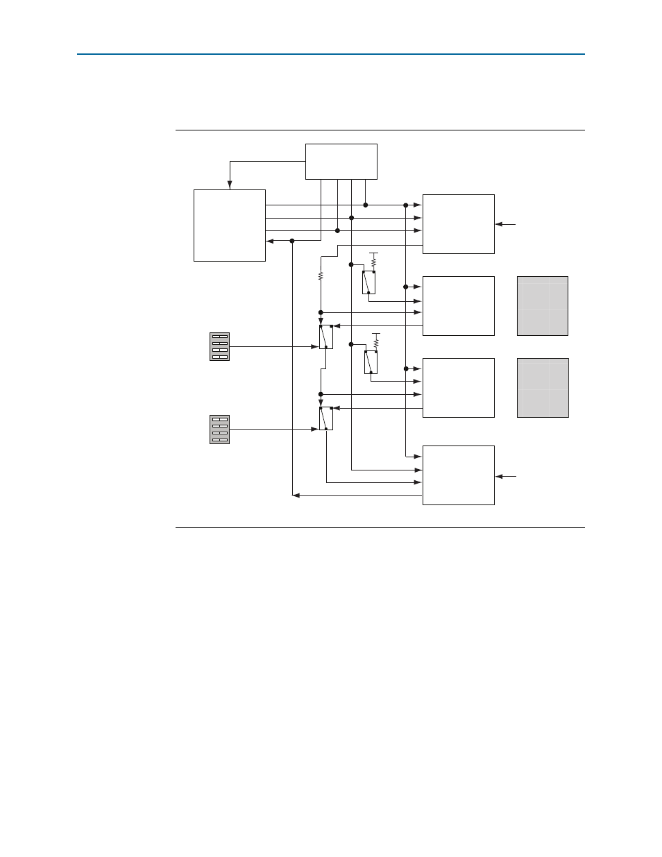
The embedded USB-Blaster II in the MAX II CPLD EPM570GT100C3N normally
masters the JTAG chain.
illustrates the JTAG chain.
The JTAG chain control DIP switch (SW3) controls the device connection. To connect a
device or interface in the chain, their corresponding switch must be in the OFF
position. Slide all the switches to the ON position to only have the FPGA and MAX V
CPLD 5M2210 System Controller in the chain.
A Cypress EZ-USB CY7C68013A device in a 56-pin VBGA package device is used to
interface to a single type-B mini-USB connector. This device has an on-board 8051
CPU used in conjunction with embedded MAC logic to translate USB data into other
formats for use by the FPGA. This CPU uses internal RAM and a small external serial
boot ROM.
Figure 2–3. JTAG Chain
Embedded
USB-Blaster II
GPIO
TCK
Cyclone V GT
FPGA
Analog
Switch
HSMC
Port A
GPIO
TMS
GPIO
TDO
GPIO
TDI
JTAG Master
GPIO
Disable
Enable
Enable
JTAG Slave
HSMC
HSMC
Port B
HSMC
TCK
TMS
TDI
TDO
TCK
2.5 V
TMS
TDI
TDO
TCK
TMS
TDI
TDO
MAX V
System
Controller
JTAG Slave
TCK
TMS
TDI
TDO
JTAG Slave
JTAG Slave
Analog
Switch
Always
Enabled
(in JTAG chain)
DIP Switch
DIP Switch
10-pin
JTAG Header
Always
Enabled
(in JTAG chain)
2.5 V