Character lcd, Components and interfaces, Pci express – Altera Cyclone V GT FPGA Development Board User Manual
Page 32: Character lcd –24, Components and interfaces –24, Pci express –24
2–24
Chapter 2: Board Components
Components and Interfaces
Cyclone V GT FPGA Development Board
September 2014
Altera Corporation
Reference Manual
Character LCD
The development board includes a single 10-pin 0.1" pitch single-row header that
interfaces to a 2 line × 16 character character LCD. The character LCD has a 10-pin
receptacle that mounts directly to the board's 10-pin header, so it can be easily
removed for access to components under the display. You can also use the header for
debugging or for I
2
C expansion.
summarizes the character LCD pin assignments.
f
For more information such as timing, character maps, interface guidelines, and other
documents related to the character LCD,
Components and Interfaces
This section describes the development board's communication ports and interface
cards relative to the Cyclone V GT device. The development board supports the
following communication ports:
■
PCI Express
■
10/100/1000 Ethernet
■
HSMC
■
SDI video output/input
PCI Express
The Cyclone V GT FPGA development board is designed to fit entirely into a PC
motherboard with a ×4 PCI Express slot that can accommodate a full height short
form factor add-in card. This interface uses the Cyclone V GT's PCI Express hard IP
block, saving logic resources for the user logic application. The PCI express edge
connector has a presence detect feature to allow the motherboard to determine if a
card is installed.
f
For more information on using the PCI Express hard IP block, refer to the
The PCI Express interface supports auto-negotiating channel width from ×1 to ×4 by
using Altera's PCIe MegaCore IP. You can also configure this board to a ×1 or ×4
interface through a DIP switch that connects the PRSNTn pins for each bus width.
The PCI Express interface has a connection speed of 2.5 Gbps/lane for a maximum of
20 Gbps in full-duplex (Gen1) and 5.0 Gbps/lane for a maximum of 40 Gbps in
full-duplex (Gen2).
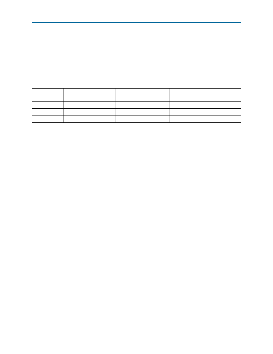
Table 2–19. Character LCD Pin Assignments, Schematic Signal Names, and Functions
Board
Reference (J10)
Schematic Signal Name
Cyclone V GT
Pin Number
I/O Standard
Description
5
DISP_SPISS
AH13
2.5-V
SPI slave select (only used in SPI mode)
7
DISP_I2C_SCL
AL6
2.5-V
I
2
C LCD serial clock
8
DISP_I2C_SDA
AJ10
2.5-V
I
2
C LCD serial data