Board overview, Board overview –2, Figure 2–1 – Altera Cyclone V GT FPGA Development Board User Manual
Page 10: Table 2–1
2–2
Chapter 2: Board Components
Board Overview
Cyclone V GT FPGA Development Board
September 2014
Altera Corporation
Reference Manual
Board Overview
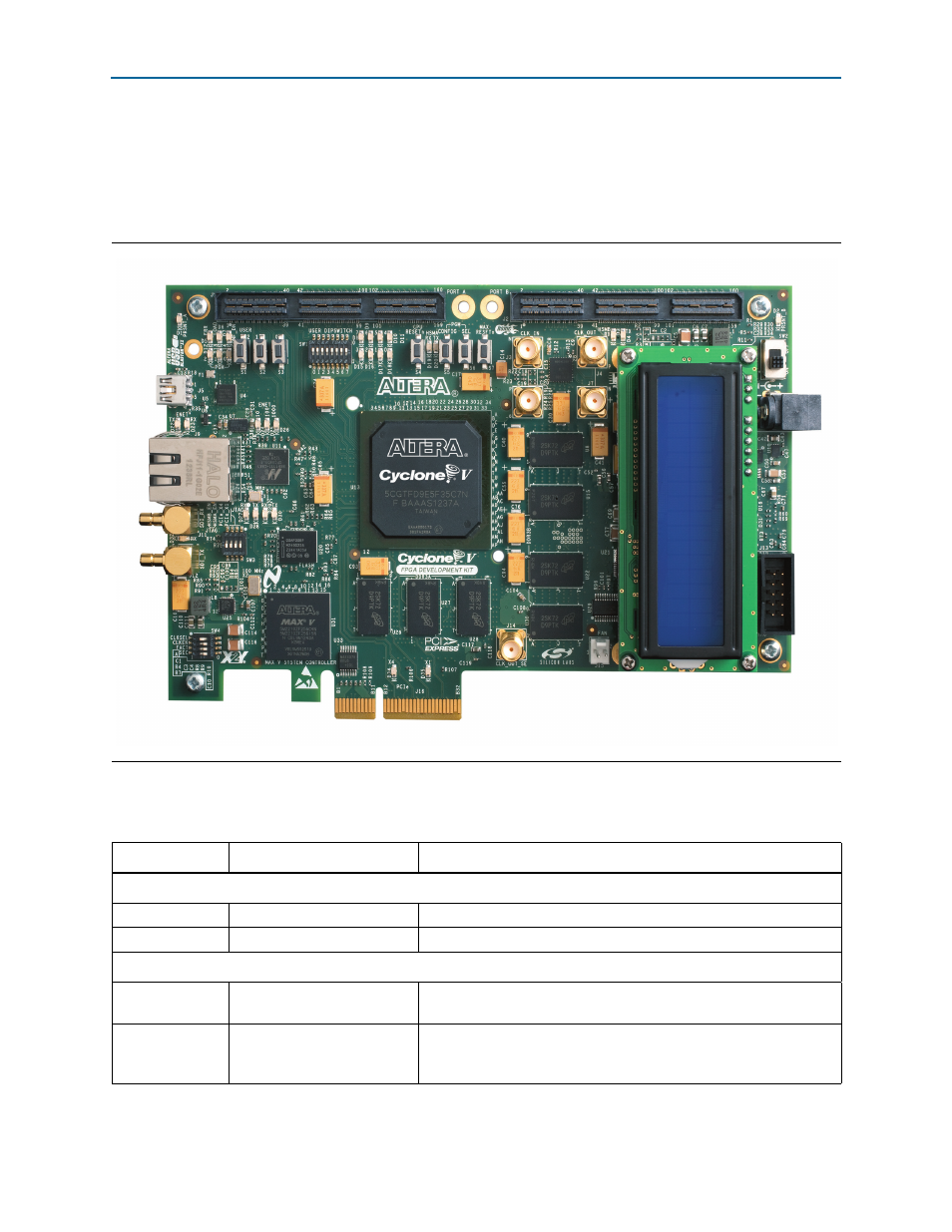
This section provides an overview of the Cyclone V GT FPGA development board,
including an annotated board image and component descriptions.
shows
an overview of the board features.
describes the components and lists their corresponding board references.
Figure 2–1. Overview of the Cyclone V GT FPGA Development Board Features
Table 2–1. Board Components (Part 1 of 4)
Board Reference
Type
Description
Featured Devices
U13
FPGA
Cyclone V GT, 5CGTFD9E5F35C7N, 1152-pin FBGA.
U32
CPLD
MAX V CPLD, 5M2210ZF256C4N, 256-pin FBGA.
Configuration, Status, and Setup Elements
J13
JTAG chain header
Provides access to the JTAG chain and disables the embedded
USB-Blaster II when using an external USB-Blaster cable.
SW3
JTAG chain control or
PCI Express DIP switch
Remove or include devices in the active JTAG chain. Also controls the
PCI Express lane width by connecting the prsnt pins together on the
PCI Express edge connector.