General user input/output, User-defined push buttons, General user input/output –21 – Altera Cyclone V GT FPGA Development Board User Manual
Page 29: User-defined push buttons –21
Chapter 2: Board Components
2–21
General User Input/Output
September 2014
Altera Corporation
Cyclone V GT FPGA Development Board
Reference Manual
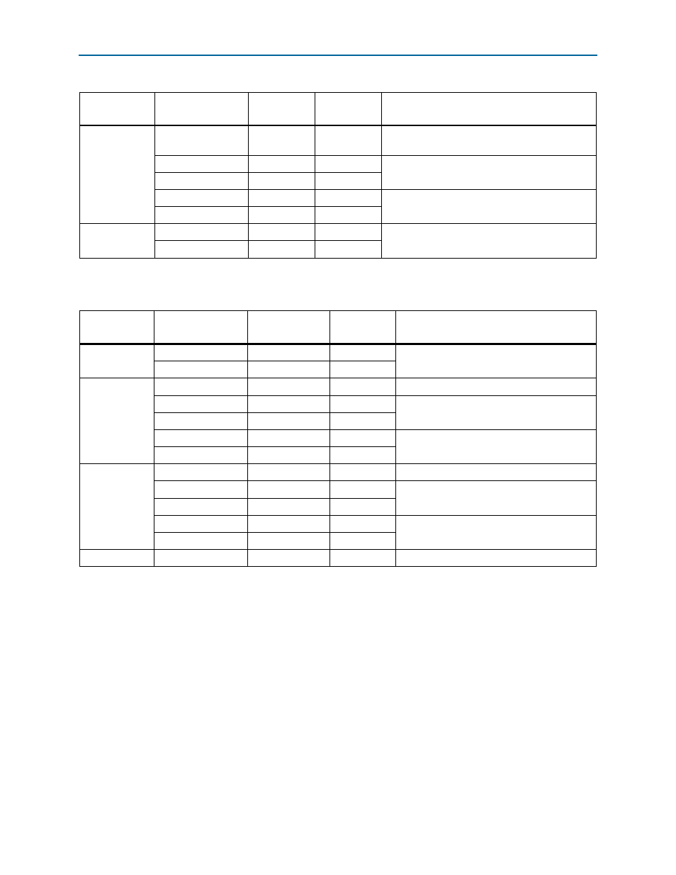
lists the clock outputs for the development board.
General User Input/Output
This section describes the user I/O interface to the FPGA, including the push buttons,
DIP switches, LEDs, and character LCD.
User-Defined Push Buttons
The development board includes three user-defined push buttons. For information on
the system and safe reset push buttons, refer to
Board references S1, S2, and S3 are push buttons for controlling the FPGA designs that
loads into the Cyclone V GT device. When you press and hold down the switch, the
device pin is set to logic 0; when you release the switch, the device pin is set to logic 1.
There are no board-specific functions for these general user push buttons.
Samtec HSMC
HSMB_CLK_IN0
2.5-V
A22
Single-ended input from the installed HSMC cable
or board.
HSMB_CLK_IN_P1
LVDS/2.5-V
K25
LVDS input from the installed HSMC cable or
board. Can also support 2x LVTTL inputs.
HSMB_CLK_IN_N1
LVDS/LVTTL
J25
HSMB_CLK_IN_P2
LVDS/LVTTL
J20
LVDS input from the installed HSMC cable or
board. Can also support 2x LVTTL inputs.
HSMB_CLK_IN_N2
LVDS/LVTTL
K19
PCI Express
Edge
PCIE_REFCLK_P
HCSL
W11
HCSL input from the PCI Express edge connector.
PCIE_REFCLK_N
HCSL
V10
Table 2–12. Off-Board Clock Inputs (Part 2 of 2)
Source
Schematic Signal
Name
I/O Standard
Cyclone V GT
Pin Number
Description
Table 2–13. Off-Board Clock Outputs
Source
Schematic Signal
Name
I/O Standard
Cyclone V GT
Pin Number
Description
LVDS SMA
CLKOUT_SMA_P
LVPECL
—
Driven from LVDS clock buffer U3
CLKOUT_SMA_N
LVPECL
—
Samtec HSMC
HSMA_CLK_OUT0
2.5V CMOS
F10
FPGA CMOS output (or GPIO)
HSMA_CLK_OUT_P1
LVDS/2.5V CMOS
C1
LVDS output. Can also support 2x CMOS
outputs.
HSMA_CLK_OUT_N1
LVDS/2.5V CMOS
B1
HSMA_CLK_OUT_P2
LVDS/2.5V CMOS
B18
LVDS output. Can also support 2x CMOS
outputs.
HSMA_CLK_OUT_N2
LVDS/2.5V CMOS
A18
Samtec HSMC
HSMB_CLK_OUT0
2.5V CMOS
D25
FPGA CMOS output (or GPIO)
HSMB_CLK_OUT_P1
LVDS/2.5V CMOS
L22
LVDS output. Can also support 2x CMOS
outputs.
HSMB_CLK_OUT_N1
LVDS/2.5V CMOS
K22
HSMB_CLK_OUT_P2
LVDS/2.5V CMOS
F26
LVDS output. Can also support 2x CMOS
outputs.
HSMB_CLK_OUT_N2
LVDS/2.5V CMOS
G26
SMA
SMA_CLKOUT
2.5V CMOS
AF33
FPGA CMOS output (or GPIO)