Figure 9-51, Ac97 data timing diagram, Table 9-41 – AMD Geode SC1201 User Manual
Page 429: Ac97 i/o timing parameters
AMD Geode™ SC1200/SC1201 Processor Data Book
429
Electrical Specifications
32579B
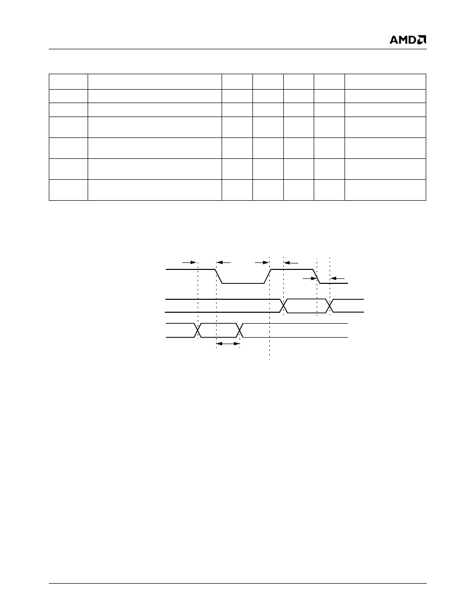
Figure 9-51. AC97 Data TIming Diagram
Table 9-41. AC97 I/O Timing Parameters
Symbol
Parameter
Min
Typ
Max
Unit
Comments
t
AC97_S
Input setup to falling edge of BIT_CLK
15.0
ns
t
AC97_H
Hold from falling edge of BIT_CLK
10.0
ns
t
AC97_OV
SDATA_OUT or SYNC valid after rising
edge of BIT_CLK
15
ns
t
AC97_OH
SDATA_OUT or SYNC hold time after
falling edge of BIT_CLK
5
ns
t
AC97_SV
Sync out valid after rising edge of
BIT_CLK
15
ns
t
AC97_SH
Sync out hold after falling edge of
BIT_CLK
5
ns
BIT_CLK
SDATA_IN, SDATA_IN2
t
AC97_S
t
AC97_H
t
AC97_OV
t
AC97_OH
t
AC97_SV
t
AC97_SH
SDATA_OUT/SYNC
This manual is related to the following products: