Table 5-38, Bank selection encoding, Table 5-39 – AMD Geode SC1201 User Manual
Page 132: Bank 1 register map, Table 5-40, Bank 2 register map, Table 5-41, Bank 3 register map
132
AMD Geode™ SC1200/SC1201 Processor Data Book
SuperI/O Module
32579B
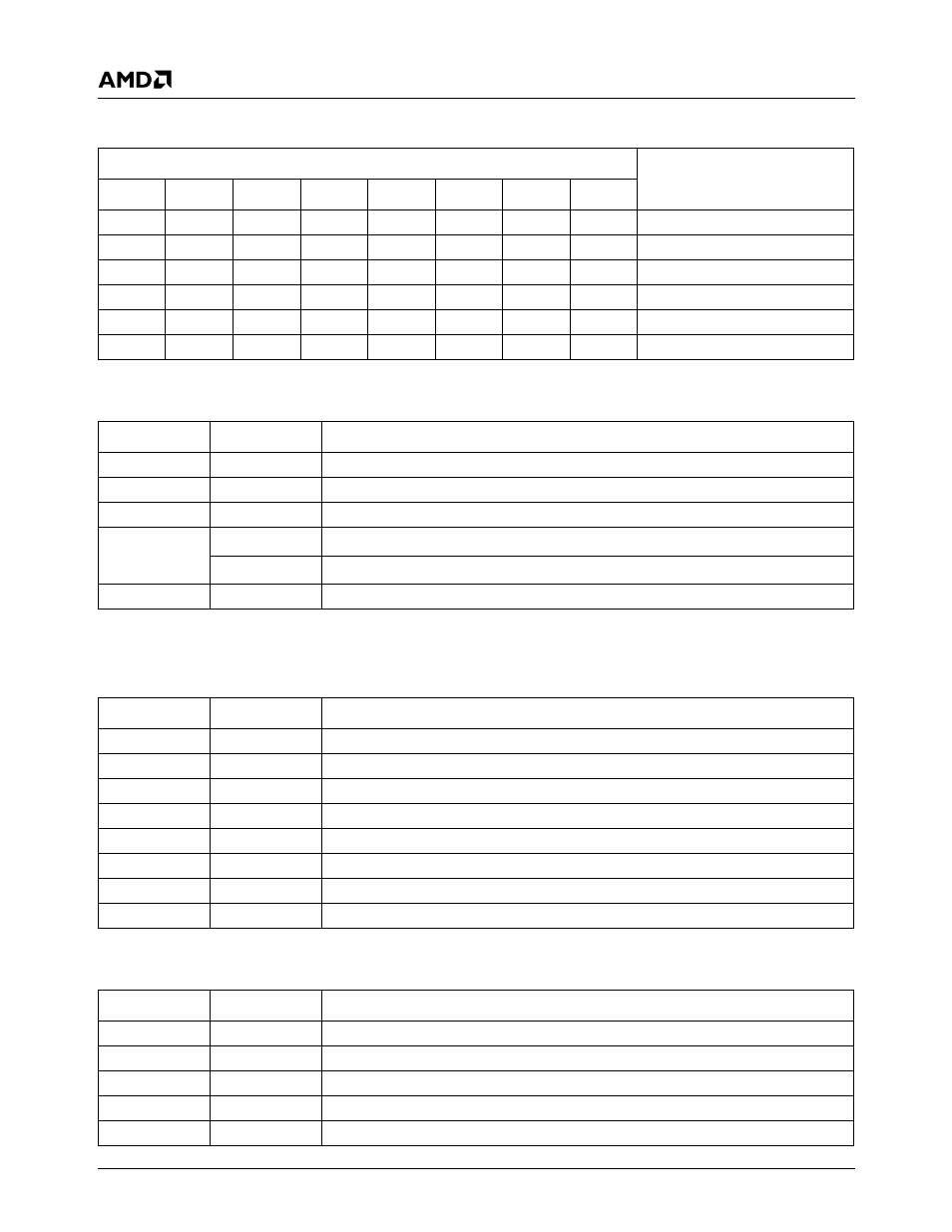
Table 5-38. Bank Selection Encoding
BSR Bits
Bank Selected
7
6
5
4
3
2
1
0
0
x
x
x
x
x
x
x
0
1
0
x
x
x
x
x
x
1
1
1
x
x
x
x
1
x
1
1
1
x
x
x
x
x
1
1
1
1
1
0
0
0
0
0
2
1
1
1
0
0
1
0
0
3
Table 5-39. Bank 1 Register Map
Offset
Type
Name
00h
R/W
LBGD(L). Legacy Baud Generator Divisor Port (Low Byte)
01h
R/W
LBGD(H). Legacy Baud Generator Divisor Port (High Byte)
02h
---
RSVD. Reserved
03h
W
LCR
1
. Line Control
R/W
BSR
1
. Bank Select
04h-07h
---
RSVD. Reserved
1.
When bit 7 of this register is set to 1, bits [6:0] of BSR select the bank, as shown in Table 5-38 on page 132.
Table 5-40. Bank 2 Register Map
Offset
Type
Name
00h
R/W
BGD(L). Baud Generator Divisor Port (Low Byte)
01h
R/W
BGD(H). Baud Generator Divisor Port (High Byte)
02h
R/W
EXCR1. Extended Control1
03h
R/W
BSR. Bank Select
04h
R/W
EXCR2. Extended Control 2
05h
---
RSVD. Reserved
06h
RO
RXFLV. RX_FIFO Level
07h
RO
TXFLV. TX_FIFO Level
Table 5-41. Bank 3 Register Map
Offset
Type
Name
00h
RO
MRID. Module and Revision ID
01h
RO
SH_LCR. Shadow of LCR
02h
RO
SH_FCR. Shadow of FIFO Control
03h
R/W
BSR. Bank Select
04h-07h
---
RSVD. Reserved