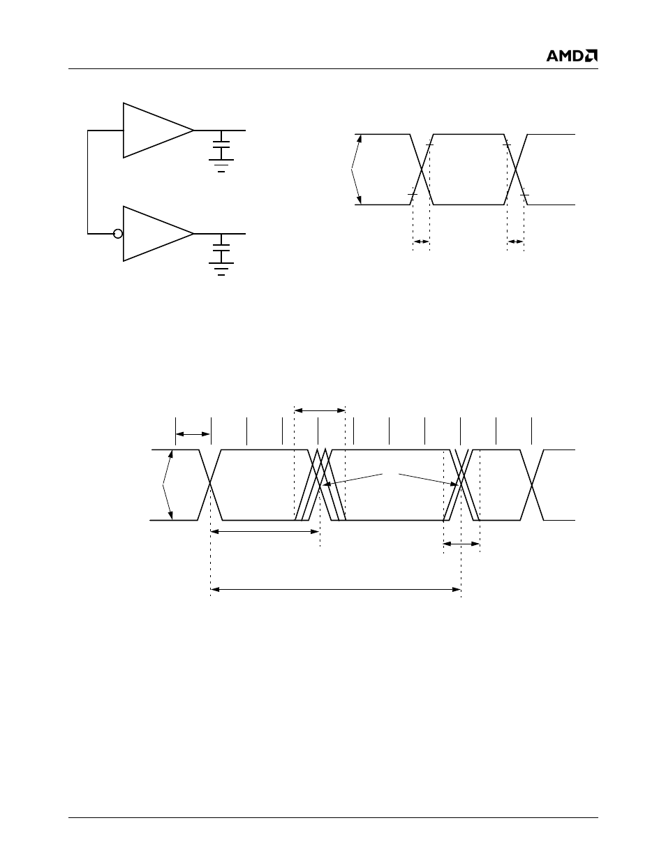
Figure 9-38, Usb data signal rise and fall timing diagram, Figure 9-39 – AMD Geode SC1201 User Manual
Page 419: Usb source differential data jitter timing diagram

AMD Geode™ SC1200/SC1201 Processor Data Book
419
Electrical Specifications
32579B
Figure 9-38. USB Data Signal Rise and Fall Timing Diagram
Figure 9-39. USB Source Differential Data Jitter Timing Diagram
Rise Time
Fall Time
t
USB_R1,2
t
USB_F1,2
90%
90%
10%
10%
Differential
Data Lines
C
L
C
L
Full Speed: 4 to 20 ns at C
L
= 50 pF
Low Speed: 75 ns at C
L
= 50 pF, 300 ns at C
L
= 350 pF
t
period_F
Paired Transitions
Consecutive Transitions
Differential
Data Lines
Crossover Points
N*t
period
_
F
+ t
USB_DJ11
N*t
period_F
+ t
USB_DJ12
(1.3-2.0) V
t
USB_DJ12
t
USB_DJ11
t
period_L
t
USB_DJD21
t
USB_DJU21
t
USB_DJD22
t
USB_DJU22
N*t
period_L
+ t
USB_DJD21
N*t
period_L
+ t
USB_DJU21
N*t
period_L
+ t
USB_DJD22
N*t
period_L
+ t
USB_DJU22
This manual is related to the following products:
