Rainbow Electronics DS2152 User Manual
Page 51

DS2152
031897 51/79
11.2 LEGACY FDL SUPP0RT
11.2.1 Overview
In order to provide backward compatibility to the older
DS2151 device, the DS2152 maintains the circuitry that
existed in the previous generation of T1 Single–Chip
Transceivers. Section 11.2 covers the circuitry and
operation of this legacy functionality. In new applica-
tions, it is recommended that the HDLC controller and
BOC controller described in Section 11.1 be used. On
the receive side, it is possible to have both the new
HDLC/BOC controller and the legacy hardware working
at the same time. However this is not possible on the
transmit side since their can be only one source the of
the FDL data internal to the device.
11.2.2 Receive Section
In the receive section, the recovered FDL bits or Fs bits
are shifted bit–by–bit into the Receive FDL register
(RFDL). Since the RFDL is 8 bits in length, it will fill up
every 2 ms (8 times 250 us). The DS2152 will signal an
external microcontroller that the buffer has filled via the
SR2.4 bit. If enabled via IMR2.4, the INT pin will toggle
low indicating that the buffer has filled and needs to be
read. The user has 2 ms to read this data before it is lost.
If the byte in the RFDL matches either of the bytes pro-
grammed into the RFDLM1 or RFDLM2 registers, then
the SR2.2 bit will be set to a one and the INT pin will
toggled low if enabled via IMR2.2. This feature allows
an external microcontroller to ignore the FDL or Fs pat-
tern until an important event occurs.
The DS2152 also contains a zero destuffer which is con-
trolled via the CCR2.0 bit. In both ANSI T1.403 and
TR54016, communications on the FDL follows a subset
of a LAPD protocol. The LAPD protocol states that no
more than 5 ones should be transmitted in a row so that
the data does not resemble an opening or closing flag
(01111110) or an abort signal (11111111). If enabled via
CCR2.0, the DS2152 will automatically look for 5 ones
in a row, followed by a zero. If it finds such a pattern, it
will automatically remove the zero. If the zero destuffer
sees six or more ones in a row followed by a zero, the
zero is not removed. The CCR2.0 bit should always be
set to a one when the DS2152 is extracting the FDL.
More on how to use the DS2152 in FDL applications in
this legacy support mode is covered in a separate
Application Note.
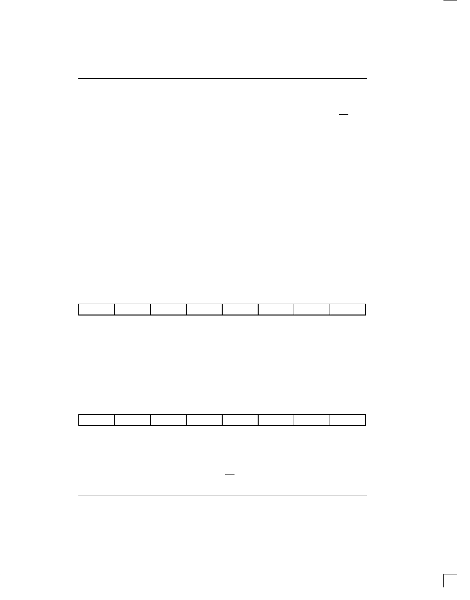
RFDL: RECEIVE FDL REGISTER (Address=28 Hex)
(MSB)
(LSB)
RFDL7
RFDL6
RFDL5
RFDL4
RFDL3
RFDL2
RFDL1
RFDL0
SYMBOL
POSITION
NAME AND DESCRIPTION
RFDL7
RFDL.7
MSB of the Received FDL Code
RFDL0
RFDL.0
LSB of the Received FDL Code
The Receive FDL Register (RFDL) reports the incoming Facility Data Link (FDL) or the incoming Fs bits. The LSB is
received first.
RFDLM1: RECEIVE FDL MATCH REGISTER 1 (Address=29 Hex)
RFDLM2: RECEIVE FDL MATCH REGISTER 2 (Address=2A Hex)
(MSB)
(LSB)
RFDL7
RFDL6
RFDL5
RFDL4
RFDL3
RFDL2
RFDL1
RFDL0
SYMBOL
POSITION
NAME AND DESCRIPTION
RFDL7
RFDL.7
MSB of the FDL Match Code
RFDL0
RFDL.0
LSB of the FDL Match Code
When the byte in the Receive FDL Register matches either of the two Receive FDL Match Registers
(RFDLM1/RFDLM2), RSR2.2 will be set to a one and the INT will go active if enabled via IMR2.2.
