Rainbow Electronics DS2152 User Manual
Page 11

DS2152
031897 11/79
RCLKI pins. Tie high to connect the the line interface cir-
cuitry to the framer/formatter circuitry and deactivate
the TPOSI/TNEGI/TCLKI/RPOSI/RNEGI/RCLKI pins.
When LIUC is tied high, the TPOSI/TNEGI/TCLKI/
RPOSI/RNEGI/RCLKI pins should be tied low.
Receive Tip and Ring [RTIP & RRING]. Analog inputs
for clock recovery circuitry. These pins connect via a 1:1
transformer to the T1 line. See Section 14 for details.
Transmit Tip and Ring [TTIP & TRING]. Analog line
driver outputs. These pins connect via a 1:1.15 or
1:1.36 step–up transformer to the T1 line. See Section
14 for details.
SUPPLY PINS
Digital Positive Supply [DVDD]. 5.0 volts
±
5%.
Should be tied to the RVDD and TVDD pins.
Receive Analog Positive Supply [RVDD]. 5.0 volts
±
5%. Should be tied to the DVDD and TVDD pins.
Transmit Analog Positive Supply [TVDD]. 5.0 volts
±
5%. Should be tied to the RVDD and DVDD pins.
Digital Signal Ground [DVSS]. Should be tied to the
RVSS and TVSS pins.
Receive Analog Signal Ground [RVSS]. 0.0 volts.
Should be tied to the DVSS and TVSS pins.
Transmit Analog Ground [TVSS]. 0.0 volts. Should
be tied to the RVSS and DVSS pins.
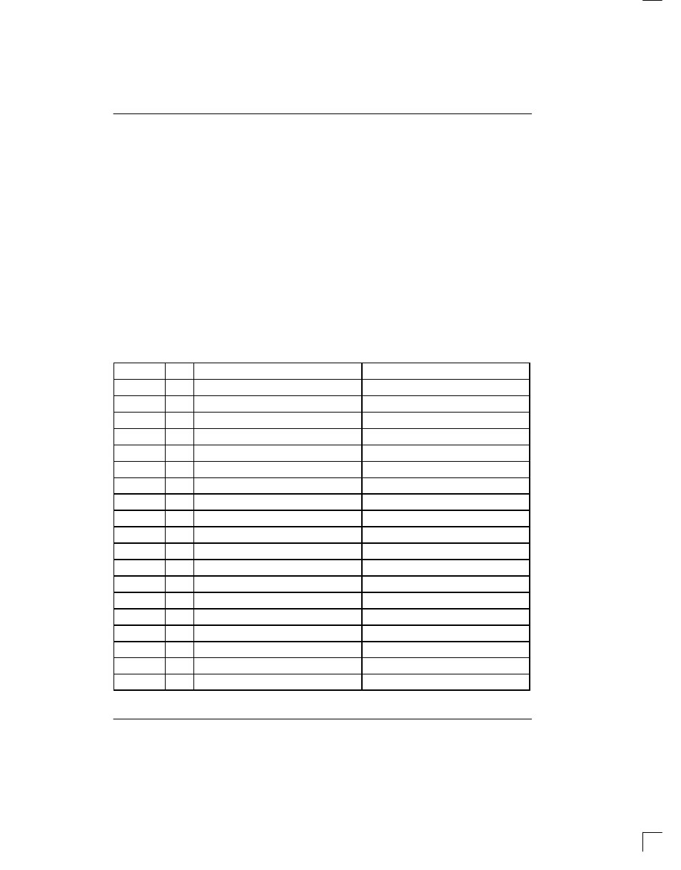
DS2152 REGISTER MAP Table 1–3
ADDRESS
R/W
REGISTER NAME
REGISTER ABBREVIATION
00
R/W
FDL Control
FDLC
01
R/W
FDL Status
FDLS
02
R/W
FDL Interrupt Mask
FIMR
03
R/W
Receive Performance Report Message
RPRM
04
R/W
Receive Bit Oriented Code
RBOC
05
R
Receive FDL FIFO
RFFR
06
R/W
Transmit Performance Report Message
TPRM
07
R/W
Transmit Bit Oriented Code
TBOC
08
W
Transmit FDL FIFO
TFFR
09
R/W
Test 2
TEST2 (set to 00h)
0A
R/W
Common Control 7
CCR7
0B
–
not present
–
0C
–
not present
–
0D
–
not present
–
0E
–
not present
–
0F
R
Device ID
IDR
10
R/W
Receive Information 3
RIR3
11
R/W
Common Control 4
CCR4
12
R/W
In–Band Code Control
IBCC
