Rainbow Electronics DS2152 User Manual
Page 41
DS2152
031897 41/79
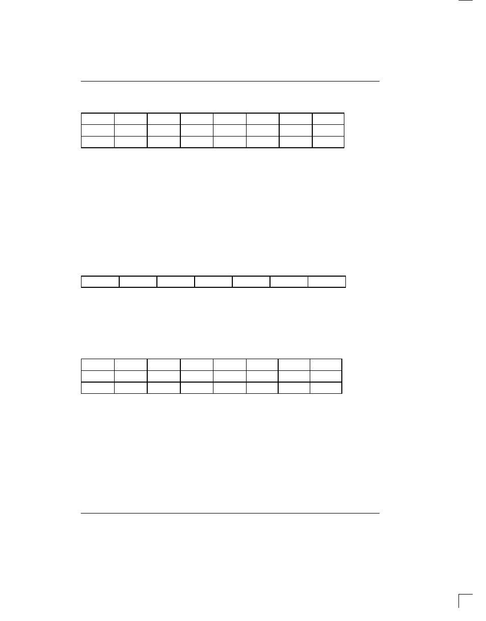
RMR1/RMR2/RMR3: RECEIVE MARK REGISTERS (Address=2D to 2F Hex)
(MSB)
(LSB)
CH8
CH7
CH6
CH5
CH4
CH3
CH2
CH1
CH16
CH15
CH14
CH13
CH12
CH11
CH10
CH9
CH24
CH23
CH22
CH21
CH20
CH19
CH18
CH17
SYMBOL
POSITION
NAME AND DESCRIPTION
CH24
RCBR3.7
Receive Channel Blocking Registers.
0 = do not affect the receive data associated with this channel
CH1
RCBR1.0
1 = replace the receive data associated with this channel with either the idle
code or the digital milliwatt code (depends on the RCR2.7 bit)
8.2.2
Per–Channel Code Insertion
The second method involves using the Receive Chan-
nel Control Registers (RCC1/2/3) to determine which of
the 24 T1 channels off of the T1 line and going to the
backplane should be overwritten with the code placed in
the Receive Channel Registers (RC1 to RC24). This
method is more flexible than the first in that it allows a
different 8–bit code to be placed into each of the 24 T1
channels.
RC1 TO RC24: RECEIVE CHANNEL REGISTERS (Address=58 to 5F and 80 to 8F Hex)
(for brevity, only channel one is shown; see Table 1–3 for other register address)
(MSB)
(LSB)
C7
C6
C5
C4
C3
C2
C0
SYMBOL
POSITION
NAME AND DESCRIPTION
C7
RC1.7
MSB of the Code (this bit is sent first to the backplane)
C0
RC1.0
LSB of the Code (this bit is sent last to the backplane)
RCC1/RCC2/RCC3: RECEIVE CHANNEL CONTROL REGISTER (Address=18 to 1D Hex)
(MSB)
(LSB)
CH8
CH7
CH6
CH5
CH4
CH3
CH2
CH1
CH16
CH15
CH14
CH13
CH12
CH11
CH10
CH9
CH24
CH23
CH22
CH21
CH20
CH19
CH18
CH17
SYMBOL
POSITION
NAME AND DESCRIPTION
CH24
RCC3.7
Receive Channel 24 Code Insertion Control Bit
0=do not insert data from the RC24 register into the receive data stream
1 = insert data from the RC24 register into the receive data stream
CH1
RCC1.0
Receive Channel 1 Code Insertion Control Bit
0=do not insert data from the RC1 register into the receive data stream
1 = insert data from the RC1 register into the receive data stream
TCC1 (16)
TCC2 (17)
TCC3 (18)
RC1 (58)
RCC1 (1B)
RCC2 (1C)
RCC3 (1D)