Hardware, Control registers – Renesas 4514 User Manual
Page 99
1-86
HARDWARE
4513/4514 Group User’s Manual
Selected pins
A
IN0
A
IN1
A
IN2
A
IN3
A
IN4
(Not available for the 4513 Group)
A
IN5
(Not available for the 4513 Group)
A
IN6
(Not available for the 4513 Group)
A
IN7
(Not available for the 4513 Group)
This bit has no function, but read/write is enabled.
Instruction clock signal divided by 8
Instruction clock signal divided by 4
Input ports P2
0
, P2
1
, P2
2
selected
Serial I/O ports S
CK
, S
OUT
, S
IN
/input ports P2
0
, P2
1
, P2
2
selected
External clock
Internal clock (instruction clock divided by 4 or 8)
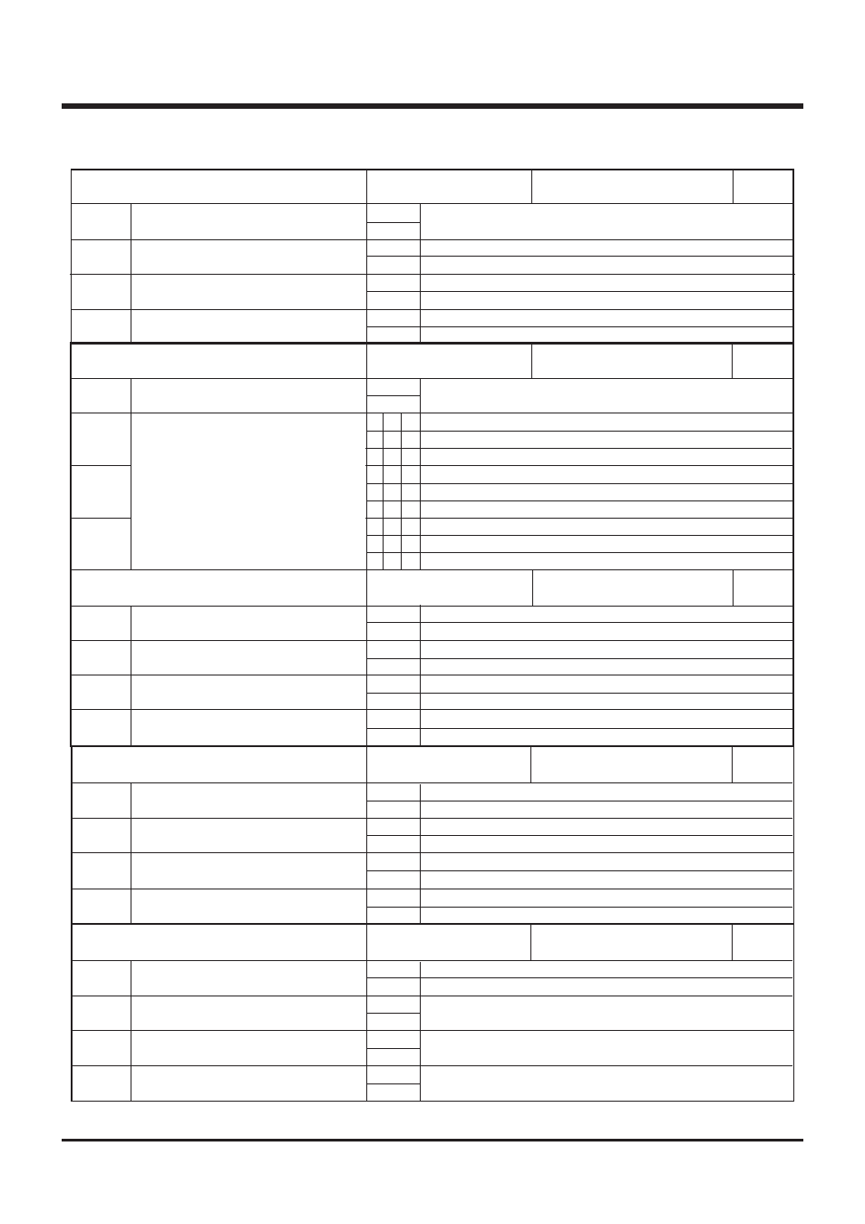
J1
3
J1
2
J1
1
J1
0
Serial I/O mode register J1
Not used
Serial I/O internal clock dividing ratio
selection bit
Serial I/O port selection bit
Serial I/O synchronous clock selection bit
at reset : 0000
2
at RAM back-up : state retained
0
1
0
1
0
1
0
1
R/W
Q1
3
Q1
2
Q1
1
Q1
0
A-D control register Q1
Note used
Analog input pin selection bits (Note 2)
at reset : 0000
2
at RAM back-up : state retained
0
1
Q1
2
0
0
0
0
1
1
1
1
Q1
1
0
0
1
1
0
0
1
1
This bit has no function, but read/write is enabled.
at reset : 0000
2
Q2
3
Q2
2
Q2
1
Q2
0
A-D control register Q2
A-D conversion mode
Comparator mode
P4
3
, P4
2
(read/write enabled for the 4513 Group)
A
IN7
, A
IN6
/P4
3
, P4
2
(read/write enabled for the 4513 Group)
P4
1
(read/write enabled for the 4513 Group)
A
IN5
/P4
1
(read/write enabled for the 4513 Group)
P4
0
(read/write enabled for the 4513 Group)
A
IN4
/P4
0
(read/write enabled for the 4513 Group)
A-D operation mode selection bit
P4
3
/A
IN7
and P4
2
/A
IN6
pin function selec-
tion bit (Not used for the 4513 Group)
P4
1
/A
IN5
pin function selection bit
(Not used for the 4513 Group)
P4
0
/A
IN4
pin function selection bit
(Not used for the 4513 Group)
at RAM back-up : state retained
0
1
0
1
0
1
0
1
Notes 1: “R” represents read enabled, “W” represents write enabled.
2: Select A
IN4
–A
IN7
with register Q1 after setting register Q2.
3: Bits 0 and 1 of register Q3 can be only read.
Q1
0
0
1
0
1
0
1
0
1
R/W
R/W
MR
3
MR
2
MR
1
MR
0
Clock control register MR
f(X
IN
) (high-speed mode)
f(X
IN
)/2 (middle-speed mode)
This bit has no function, but read/write is enabled.
This bit has no function, but read/write is enabled.
This bit has no function, but read/write is enabled.
System clock selection bit
Not used
Not used
Not used
at reset : 1000
2
at RAM back-up : 1000
2
0
1
0
1
0
1
0
1
R/W
Q3
3
Q3
2
Q3
1
Q3
0
Comparator control register Q3 (Note 3)
at reset : 0000
2
at RAM back-up : state retained
0
1
0
1
0
1
0
1
R/W
Voltage comparator (CMP1) invalid
Voltage comparator (CMP1) valid
Voltage comparator (CMP0) invalid
Voltage comparator (CMP0) valid
CMP1- > CMP1+
CMP1- < CMP1+
CMP0- > CMP0+
CMP0- < CMP0+
Voltage comparator (CMP1) control bit
Voltage comparator (CMP0) control bit
CMP1 comparison result store bit
CMP0 comparison reslut store bit
CONTROL REGISTERS